Skip to main content
Mobile menu
Discover
Develop
Agile
Resources & Support
Free Altium 365 Tools
Gerber Compare
Online PCB Viewer
Resources & Support
Learning Hub
Support Center
Documentation
Webinars
Altium Community
Forum
Bug Crunch
Ideas
Education
Student Lab
Educator Center
Altium Education Curriculum
Search Open
Search
Search Close
Sign In
Main menu
Home
PCB Design
Collaboration
Component Creation
Data Management
Design Outputs
ECAD/MCAD
HDI Design
High Speed Design
Multi-Board
PCB Layout
PCB Routing
PCB Supply Chain
Power Integrity
RF Design
Rigid Flex
Schematic Capture
Signal Integrity
Simulation
Software
Develop
Discover
Agile
Altium 365
Altium Designer
Education
Programs
Altium Academy
Engineering News
Guide Books
Newsletters
Podcasts
Projects
Training Courses
Webinars
Whitepapers
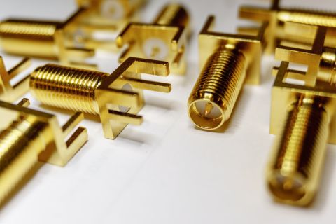
PCB Mountable Connectors: SMD vs. Through-hole
When I designed some of my first boards, I was always working at DC or low speed, and any signal integrity problems from my connectors were an afterthought. These initial boards were for low frequency measurements of an electrochemical sensor. The only circuitry involved was a low-pass filter circuit with through-hole passives, a PCB mountable connector for a lab-grade power supply, and a parallel connection to an SMU. After learning the finer
Read Article
Designing Pressure Tolerant Electronics: It's All About Mechanics
After a recent inquiry from a customer about a high power board that must withstand high gas pressures, my team suddenly realized we needed to do some research on designing pressure tolerant electronics. This area is not as popular as designing electronics for ambient pressures, but the design techniques used here enable important scientific expeditions and industrial applications in high pressure environments. Whether the board will be placed in
Read Article
High Voltage SMPS PCB Layout to Minimize Heat and Noise
Whether you are performing AC-DC conversion or DC-DC conversion, switching power supply layouts are common in high voltage design and must be constructed carefully. Although this system is quite common, it will easily radiate EMI due to the fast changes in voltage and current during switching. Designers can rarely adapt existing designs into new systems as a minor change in one area can create an EMI problem that is difficult to diagnose. With
Read Article
How to Select an Inductor for a Buck Converter
An SMPS is one of those quiet (yet electrically noisy) devices that makes your favorite electronics run smoothly. They sit in the background quietly doing their duty, yet your board wouldn’t operate without them. As part of DC-DC converter design for power-hungry applications, component selection is quite important for ensuring stable power delivery to a load with high efficiency. Among the numerous DC-DC converter topologies, a buck converter
Read Article
Driving Haptic Vibration and Feedback in Wearables
Augmented reality, virtual surgery, limb replacements, medical devices, and other new technologies need to incorporate haptic vibration motors and feedback to give the wearer a full sense of how they are interacting with their environment. Unless these cutting-edge applications include haptic vibration and feedback, users are forced to rely on their other four senses to understand the real or virtual environment. Low cost components to support
Read Article
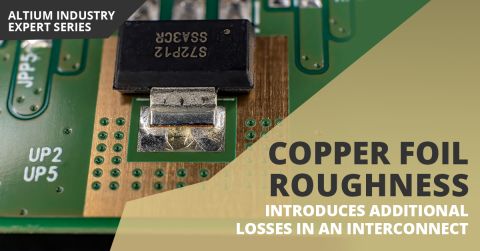
Modeling Copper Foil Roughness in Altium Designer's Impedance Profiler
Advanced transmission line models for long interconnects require that designers include copper foil roughness calculations in order to determine accurate impedance. Without the right models or design software, you’ll be left to estimate the skin effect impedance, dispersion, and parasitics in your PCB. These models can be difficult to work with by hand if you’re not mathematically inclined, but the right design tools can be used to quickly
Read Article
High-Speed Signal Routing: The 5 Important PCB Design Constraints
Your modern digital board is most likely classified as high speed, regardless of whether you looked at the datasheets for your components. Designing your board successfully will take some important steps when you begin your design. Aside from floorplanning and stackup design, your routing strategy will need to operate within some important PCB design constraints. After you capture your schematic as an initial layout and create an initial
Read Article
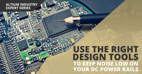
How to Reduce Clock and Signal Jitter: Debugging Power Supply Noise
Low level components need ultra-stable power, and high speed digital signals need to have repeatable edge transition times. The two aspects of digital signalling are related, and you’ll need to suppress all aspects of power supply noise to reduce jitter in a digital system. During a design debug, you’ll need to gather measurements throughout your board if you want to isolate and eliminate sources of power supply noise. Here’s how you can isolate
Read Article
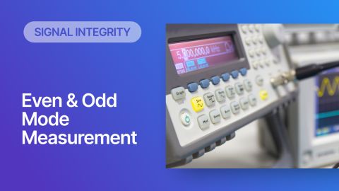
Transmission Line Impedance Measurement: Even vs. Odd Mode
If you need an accurate transmission line impedance measurement, here are the important values you need to use in your next board.
Read Article
How to Take a Phase Noise Measurement in a PCB
There are plenty of noise sources in your PCB, ranging from thermal noise to EMI received from external sources. Phase noise is one noise source that occurs in analog signal sources like reference oscillators and frequency synthesizers. This type of noise affects the timing of analog signals and it arises due to contributions from other noise sources. If you’re debugging a high frequency board with a reference oscillator, then you might need to
Read Article
Pagination
First page
« First
Previous page
‹ Previous
…
Page
181
Page
182
Page
183
Page
184
Current page
185
Page
186
Page
187
Page
188
Page
189
…
Page
190
Page
200
Page
210
Page
220
Page
230
Page
240
Page
250
Page
260
Page
270
Page
280
Page
380
Next page
Next ›
Last page
Last »
Subscribe to