Round and Curved PCB Design in Altium Designer

Our modern lives would not be possible without electronics. Sometimes it seems like a race to be the first person to wire everything in your house onto PCBs. With the multitude of possible device shapes and sizes, circular or rounded PCBs are becoming more popular. If you want to design your next device on a round PCB, your design software needs CAD and layout tools that don’t constrain you to working on rectangular PCBs. When you work with Altium Designer, you’ll have full control over your PCB footprint and layout, and you can build PCBs with any shape or size.
ALTIUM DESIGNER
A PCB design software package with the best PCB layout tools for curved or round PCBs.
As PCBs take on stranger form factors and require more advanced capabilities, your design strategies need to keep up with these changes. If your next electronic device has a round form factor, using a round PCB can give you more board space and might be preferable over using multiple rectangular boards. You’ll likely need to implement a number of other design rules and strategies for your particular application. Using an excellent PCB design software package with the best CAD and layout tools will make designing your next round PCB a breeze.
Round and Curved Design Strategies
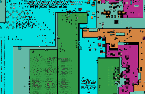
Once you’ve decided on a shape for your PCB, you’ll need to draw out the shape of your board in your CAD tool. This forms the foundation for your board, and you can then proceed to lay out components. If you’re working on a high-performance device, you’ll likely be designing a multilayer PCB with high-speed or high-frequency capabilities. You’ll also need to define ground and power planes in different layers. Defining the shape of your power/ground layers requires a polygon editor that is built into your design software.
Round PCB Design for Specific Applications
Certain applications require curved or round devices, and it can pay to design your PCB to match the form factor of your device packaging. Using a rectangular board inside a curved package reduces available board space, and working with curved designs allows your PCB to match the contour of your packaging. This gives you more design flexibility and can even allow you to expand your design to include new features in the future.
- Specific boards shapes require great CAD tools for different applications. Great design software makes building curved and round PCBs easy. Learn more about customizing your board shape for specific applications.
- Defining your power and ground planes in a curved or round PCB requires design software with a polygon editor. This lets you customize your ground and power planes so that they can fit your round PCB. Learn more about customizing ground and power planes in your PCB.
- Excellent CAD and layout tools make it easy to include complex board and pad shapes in your PCBs.See more tips for creating complex designs for your PCBs.

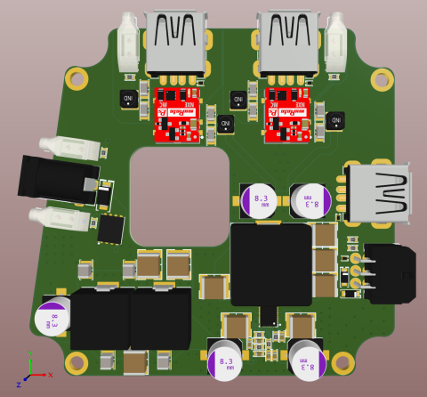
Curved board design in Altium Designer
Curved and Round PCBs for Wearable and IoT Devices
Wearable and IoT devices can take on rather odd form factors. This is especially true with wearable devices, and most wearables require rigid-flex curved or round PCBs. The amount of real estate available on these boards is already low, but using a curved PCB will help you maximize your board space. The right PCB design software package will help you ensure that you can add all the electronic capabilities you need for your next wearable or IoT device.
Design Your Next Wearable or IoT Device with the Best PCB Design Software
With wearable and IoT devices requiring so many high-performance features in such a small footprint, design simulation, layer stackup, polygon design, and rules checking features become critical. Integrating round PCB design with other standard design features requires PCB design software that unifies these features in a single interface. Your circuit board will be grateful that you’ve used printed circuit technology for smart board outline and holes placement.
- You’ll need to decide whether to include solid planes or odd-shaped polygons in your PCB for ground and power. Your design software should include standard and customizable via options. Learn more about designing with polygons and planes in your PCB.
- If you’re designing a PCB for use in a wearable device, you’ll likely be using a rigid-flex design with an odd-shaped board. Learn more about wearable PCB design techniques.
- IoT devices also use odd-shaped boards with high performance. These devices often integrate round PCB and rigid-flex design techniques. Learn more about using round PCBs in IoT design.
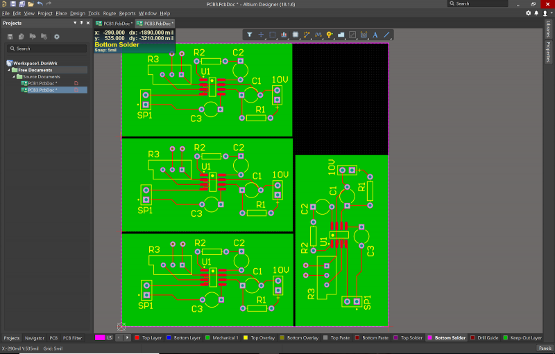
Custom panelization in Altium Designer
Moving From Design to Manufacturing with Altium Designer
Altium Designer gives you access to the best CAD tools for defining your board shape and the best layout tools for designing your devices. Since most boards are being designed as multilayer, high speed, low power, high-frequency, or a combination of all of these, you’ll need several other tools to complete your designs. Altium Designer includes simulation and analysis tools, an intuitive layer stackup manager, and top-notch component and data management features. It’s all accessible within a single design interface.
Just like with any rectangular PCB, you’ll need to generate deliverables for your manufacturer once you decide to produce your round PCB. Curved or rounded PCBs require unique panelization schemes and detailed milling instructions, in addition to the standard PCB manufacturing and assembly outputs. Altium Designer will generate your panelization instructions, bills of materials, and Gerber files for your manufacturer within a unified design environment.
Get Access to the Best PCB Design Features in Altium Designer
Using piecemeal design software is a great way to kill your productivity. Instead of moving between multiple modules or programs, your design software should give you the capabilities to access any of the tools you need from a single program. Altium Designer gives you the power to design fully customized PCBs and all within an integrated design platform.
- PCB layout requires CAD tools that let you place components with unparalleled accuracy. Altium Designer integrates your PCB layout with other critical features, giving you the power to design the best PCBs.Learn more about the design environment in Altium Designer.
- Altium Designer gives you the power to define any board shape you like with powerful CAD tools. If you can imagine it, you can design it. Learn more about defining your board shape in Altium Designer.
- Curved and round boards require unique panelization schemes. If you want to maximize your output, you’ll need to plan a unique panel arrangement for your rounded boards. Learn more about panelization in Altium Designer.
Designing unique boards is easy when you work in a unified design environment. Your design interface should integrate with trace routing, data management, and deliverable generation tools without having to move between multiple programs. You can validate your device with integrated design rule checking and simulation features, ensuring that your next round PCB design will be a success.
When you need to build a board with odd form factor and advanced capabilities, look to a great PCB design software package like Altium Designer. You’ll have access to all the tools you need to completely customize your design. You’ll have access to all the best the PCB design industry demands within Altium Designer.


