


Bend Reliability: How Trace Geometry and Materials Impact Flex Lifespan

At a Glance
Learn how trace geometry and material choices affect flex PCB bend life. Discover design rules that prevent cracking and failure.


One of the most common questions I hear when talking with designers working on designs with flexible circuits is: "How many times can this flex safely bend before it fails?" It's a fair question, especially for dynamic flex applications like wearables, medical devices, robotics, or aerospace harnesses. Unfortunately, the answer isn't as simple as a number or bend ratio, it is very dependent on the design itself and the material set.
Bend reliability is not just about the base materials themselves, but how traces are routed, the copper type and thickness, and even the way protective layers are applied. Let's look at what really drives reliability in flex circuits and what designers can do early in the process to maximize flexibility.
Key Takeaways
- Flex life depends on design, not a fixed number. Bend reliability varies widely based on whether the application is static or dynamic, and on choices like materials, routing, and bend radius.
- Copper and stackup matter most. Rolled annealed (RA) copper, thinner copper weights, adhesiveless laminates, and durable coverlays significantly improve performance in dynamic flexing.
- Smart routing reduces stress. Curved, evenly spaced traces that avoid sharp angles, perpendicular crossings, and concentrated vias dramatically increase bend durability.
- Bend radius and strain relief are critical. Larger bend radii (especially for dynamic flex) and added stiffeners or strain relief near connectors prevent premature failures and extend product life.
Static vs. Dynamic Flexing
First, there is the distinction between static and dynamic flexing:
- Static flexing occurs once or a few times. A good example is folding a flex circuit into place inside a smartphone or avionics module. Once installed, it stays put.
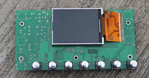
- Dynamic flexing refers to repetitive, ongoing motion. Consider a robotic arm, a folding medical device, or a wearable sensor. Such applications may require thousands or possibly millions of bend cycles over the product’s life.
Understanding which category your design falls into is critical, as it dictates the rules for trace geometry and material selection. Static applications offer much more design freedom, while dynamic flexing demands far greater control over every detail.
The Role of Copper: Rolled Annealed vs. Electrodeposited
One of the most basic decisions is copper foil type.
- Electro-deposited (ED) copper is the standard choice in rigid PCBs. It provides excellent adhesion to dielectric films, but possesses a columnar grain structure which exhibits a tendency to crack under repeated bending.
- RA copper: The mechanical working and heat treatment of rolled annealed copper generate a grain structure that is even and ductile. RA copper can flex cyclically without fracturing, which makes it a popular choice for dynamic flex designs.
For static flex, ED copper may be acceptable and can sometimes reduce cost. But for anything that moves over time, RA copper is almost always worth the investment. In addition, RA copper is most often used in commercially available flex PCBs.
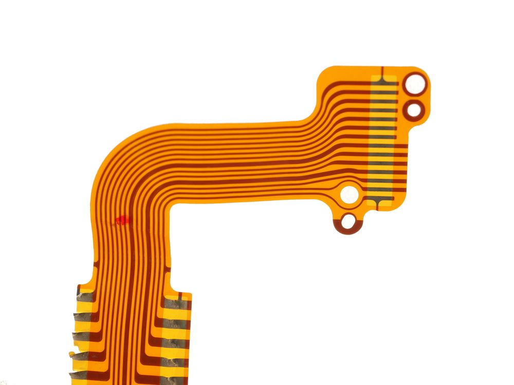
Trace Geometry and Routing Strategies
One of the key controllable factors for designers is how traces are routed in the bend area. Even small adjustments can dramatically increase reliability.
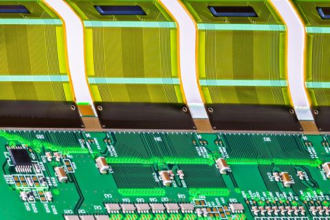
- Trace Width: Wider traces distribute stress better, but when multiple signals are needed, using several narrower traces evenly spaced is better than using one very wide trace.
- Uniform Spacing: Use consistent spacing through the bend area. Do not route traces tightly grouped to one edge of a flex; this produces uneven copper distribution, which creates stress points.
- No Perpendicular Traces: Traces crossing bends should do so at 90° only if no other route is available. Angled or curved routing distributes stress far more evenly. Best practice is to route traces perpendicular to the bend axis in static applications, and curved style routing in dynamic flex regions.
- Staggered Vias: If vias are required, don't line them up across the bend area. Stagger them to reduce stress concentration or remove them from the bend area entirely.
A general guideline is to design traces that "flow" with the bend, rather than fight it. Smooth curves always perform better than sharp corners.
Copper Thickness and Flexibility
Thicker copper is stronger electrically, but less forgiving mechanically.
- 1 oz. copper (35 µm) is common in rigid boards but is rarely suitable for repeated flexing.
- ½ oz. (18 µm) or ⅓ oz. (12 µm) copper are better choices for dynamic flex.
- In some ultra-flexible designs, ¼ oz. (9 µm) copper can be used to maximize bend life.
Where thicker copper is unavoidable, keep those layers out of the dynamic bend region and confine them to rigidized areas.
Dielectrics, Adhesives, and Coverlays
The thickness of the dielectric also plays an important role in the bend reliability: while a thinner dielectric allows tighter bend radii, it may limit the voltage isolation.
Polyimide films are the norm, and adhesives bond them to copper. Adhesiveless laminates, where the copper is directly bonded to the polyimide, may provide better reliability because there is no adhesive layer to crack and the stack up is thinner.
The choice of coverlay vs. flexible soldermask:
- Coverlays are made of polyimide plus adhesive; protect copper both mechanically and chemically, but the adhesive might creep into the pads if not designed properly.
- Flexible soldermask provides better registration for fine-pitch pads but is less durable under dynamic flexing.
For dynamic flex, coverlay is almost always the best choice due to its mechanical durability.
Bend Radius: The Design Rule That Can't Be Ignored
Every flex design has a minimum bend radius-the tightest curve it can withstand without damage. Usually this is defined as a multiple of the flex thickness:
- Static flex: 6x the flex PCB thickness is often cited as the bare minimum, with 10x being a more conservative starting point.
- Dynamic flex: Much higher value of up to 100x the flex PCB thickness may be needed for long-term durability.
For example, a 4-mil thick flex in a dynamic application should have a bend radius of ~400 mils (0.4"); trying to force a tighter bend will dramatically shorten the life of the flex. In general, a larger bend radius in dynamic flex will result in longer lifetime.
Strain Relief and Mechanical Support
The best materials and routing strategies cannot succeed if the flex circuit is allowed to move freely at connector interfaces or component areas. Stiffeners and strain relief address this issue. Also, adding FR-4 stiffeners around connectors helps to move the bend points away from the solder joints, a very common failure point.
Strain-relief features, such as fillets of epoxy or Kapton tape, help to make a smoother transition between the stiffened and flexible areas.
Wrapping It Up
Designing for bend reliability is a study in trade-offs. Thinner copper increases flexibility but can limit current carrying capacity. Rolled annealed copper improves lifespan but is more expensive. Larger bend radii extend reliability but can conflict with enclosure constraints.
It's a question of knowing what the levers are that you can pull-copper type, trace geometry, dielectric thickness, bend radius-and making conscious decisions about which to use based on whether the design is static or dynamic.
And as always, the best designs come from collaboration. Engaging your fabricator early to discuss bend requirements, material options, and testing methods will give you confidence that the final flex circuit can survive the life of your product.
Whether you need to build reliable power electronics or advanced digital systems, Altium Develop unites every discipline into one collaborative force. Free from silos. Free from limits. It’s where engineers, designers, and innovators work as one to co-create without constraints. Experience Altium Develop today!
Frequently Asked Questions
How many times can a flex circuit bend before it fails?
There is no single number. Bend life depends on whether the design is static or dynamic, along with material choices, trace routing, copper thickness, and bend radius. Dynamic flex designs can range from thousands to millions of cycles if properly engineered.
What is the difference between static and dynamic flex circuits?
Static flex circuits bend only once or a few times during installation and then remain fixed. Dynamic flex circuits bend repeatedly during operation, such as in wearables or robotics, and require stricter design rules and materials for long-term reliability.
Why is rolled annealed (RA) copper preferred for dynamic flex designs?
RA copper has a ductile grain structure that resists cracking under repeated bending, making it far more reliable than electrodeposited (ED) copper in applications with continuous or cyclic motion.
What bend radius should I use for a flex PCB?
A common guideline is at least 6–10× the flex thickness for static applications, and up to 100× the thickness for dynamic applications. Larger bend radii significantly improve flex life, especially in high-cycle designs.
What are the most common causes of flex circuit failure?
Typical failure points include tight bend radii, thick or unsuitable copper in bend areas, sharp trace corners, vias placed in bend regions, and lack of strain relief near connectors or stiffened areas.
About Author
Related Resources
Related Technical Documentation
Table of Contents
- Key Takeaways
- Static vs. Dynamic Flexing
- The Role of Copper: Rolled Annealed vs. Electrodeposited
- Trace Geometry and Routing Strategies
- Copper Thickness and Flexibility
- Dielectrics, Adhesives, and Coverlays
- Bend Radius: The Design Rule That Can't Be Ignored
- Strain Relief and Mechanical Support
- Wrapping It Up
- Frequently Asked Questions
- How many times can a flex circuit bend before it fails?
- What is the difference between static and dynamic flex circuits?
- Why is rolled annealed (RA) copper preferred for dynamic flex designs?
- What bend radius should I use for a flex PCB?
- What are the most common causes of flex circuit failure?
Design to Release, Without the Friction
- Keep reviews tied to the right version
- Reduce handoff confusion and rework
- Spot sourcing and release risk earlier
- Work solo, share when needed
Get Started
Thank you, you are now subscribed to updates.