Crosstalk Basics in PCB Design

Introduction
In this article, we will discuss the basics of crosstalk in PCB design and how to reduce crosstalk in your own designs by following simple guidelines.
Crosstalk Basics
Simply speaking, crosstalk is the unwanted transfer of energy from one element (the aggressor) to another element (the victim). These elements can be traces, components, planes, and so on.
This energy transfer happens due to capacitive and inductive coupling, as all real-world elements have some amount of parasitic and stray capacitances and inductances associated with them. For crosstalk to occur, we then require that we have changing signals (voltages and current) over time.

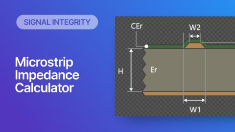
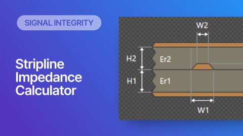
The magnitude of crosstalk between an aggressor and a victim is dependent on a variety of factors. The main factors that influence this are if the traces are routed as microstrip (external) or stripline (internal) traces, the spacing between traces and reference planes, the edge rate of a digital signal (or maximum frequency in a particular signal), voltage of the aggressor, and parallel run length.
There are a number of different forms of crosstalk, such as near-end and far-end, and I’d strongly suggest checking out Zach Peterson’s Altium Academy video covering that topic.
Excessive amounts of crosstalk may lead to, for example, erroneous ADC readings, data and timing errors (which in turn may lead to requiring a lower data rate), spurious resets, and more. Therefore, our aim as PCB designers is to mitigate crosstalk to the extent that we can.
How Much Crosstalk Can We Tolerate?
Deciding on how much crosstalk is allowed between an aggressor and victim is entirely situation-dependent. After defining system requirements, such as maximum coupled voltage on to the victim line, we can calculate, for example, how far away a particular aggressor trace needs to be, what maximum parallel runs are allowed to be, and so forth.
I would strongly suggest entering various parameter values into a freely-available crosstalk calculator and observing the results.
To give an example, we may be designing a piece of hardware that routes from an analogue sensor to a microcontroller which contains a 10-bit ADC. Assuming the microcontroller is powered from a +3.3V supply, that gives, for the ADC’s least significant bit, a voltage step of approximately 3.2mV.
Now, if we have an aggressor, such as a digital clock trace routed close to the ADC trace, we would like to know what spacing we require between these two traces to keep the ADC reading error below one least-significant bit.
In this example, the aggressor is a 10ns rise-time 3.3V signal, routed in parallel for 50mm on the same external layer as the ADC trace. Both traces are routed above a ground plane, separated by a 0.1mm thickness dielectric with a dielectric constant of 4.
Using a crosstalk calculator, we arrive at the result that the spacing needs to thus be at least 2.6mm to ensure we don’t get a one-bit error in the reading.
Crosstalk Simulation in Altium Designer
Rather than using a basic calculator, crosstalk can be very easily and quickly simulated using Altium Designer’s ‘Signal Integrity’ tool. Not only can we simulate various logic families but also import IBIS models for more accurate results.
Make sure to check out Zach Peterson’s tutorials on Altium Academy that cover crosstalk and Altium Designer’s signal integrity tool in great detail.
Reducing Crosstalk in PCB Designs
There are many ways of reducing crosstalk in PCB design. Let’s examine some tips that you can implement right away in your own PCB designs! Keep in mind there are additional methods that could lead to a reduction in crosstalk, which may not be mentioned here.
Tip #1 – Spacing
Spacing is one of the main parameters we as PCB designers have control over and one of the most effective methods of reducing crosstalk. Make sure to space out aggressors and victims to minimise crosstalk. This can even be across layers of course.

Tip #2 – Decrease Distance to Reference Planes
If you’ve played around with the crosstalk calculator or signal integrity tools, you may have noticed that decreasing the distance from traces to reference planes typically decreases the crosstalk magnitude as well. This is due to the fact that the electromagnetic fields spread out less, are better contained in the dielectric material between trace and plane, and in turn there is less coupling.

Tip #3 – Avoid Adjacent Signal Layers (if possible)
I typically recommend against having two adjacent signal layers in your PCB stack-up. If this is unavoidable however in your particular design, aim to route signal traces on one layer in horizontal directions, and traces on the other layer in vertical directions.

Tip #4 – Reducing Lengths of Parallel Routes
Reducing parallel length of runs can be effective in some cases. However, usually backward crosstalk dominates and reaches a significant magnitude after only very short parallel lengths and thus is difficult to avoid.
Additionally, in many scenarios, such as wide DDR memory interface, longer parallel runs are unavoidable.

Tip #5 – Termination
Termination, in certain cases, can improve crosstalk behaviour by reducing higher-frequency artefacts such as ringing, or even slowing down edges. However, this is very situation-dependent and should not be applied without proper reasoning, calculation, and simulation.

Outro
We examined the basics of crosstalk, looked at what parameters influence crosstalk magnitudes, and how we can apply simple guidelines to our own PCB designs to reduce crosstalk.
Keep in mind that we are only scratching the surface and there is a lot more to crosstalk. Make sure to check out Altium Designer’s Signal Integrity tool and Altium Academy videos to go in-depth on PCB design and crosstalk!


