Multi-Board PCB Signal Integrity: A Complete Guide

At a Glance
Multi-board PCB assemblies must adhere to signal integrity rules and ensure low EMI. These two aspects are intertwined, as explained in this comprehensive guide.


Multi-board PCB design sounds very simple on the surface. You're designing an assembly of multiple boards and linking them together with cables, edge connections, mezzanine connectors, pogo pins, etc. Multi-board PCBs have a set of signal integrity connectors challenges that are not always found in systems that only have a single PCB. Whether you have a single board or an assembly of multiple boards, signal integrity needs to be maintained, especially in advanced systems found in areas like military, aerospace, HPC, and AI.
Where, then, does one apply signal integrity connectors principles in a multiple PCB assembly? There are a few areas where signal integrity needs to be maintained and often qualified experimentally:
- Connector pinouts and interfaces
- Cable assemblies and harness designs
- Connections back to an enclosure, e.g., a metalized enclosure
Signal integrity connector problems in these areas can also turn into EMI/EMC problems, and that is especially true in multi-board PCBs.
In this guide, I'll aim to illustrate how to select components and design interconnects such that multi-board signal integrity is maintained. These steps still don't eliminate the need for on-PCB signal integrity; both areas are important in the systems and help prevent EMI problems.
Signals and Emissions on Multi-Board Interconnects
When referring to multi-board PCB design, obviously, we are transferring signals between two PCBs, so we should know something about the signals and the potential emissions they can create. This reference to emissions is one of the core links between EMI/EMC and multi-board PCB design.
The type of emissions and noise you can expect depends on the type of signal you need to send between two PCBs:
- Differential signals, which are self-referencing
- Single-ended signals, which require a reference
- Sinusoidal or narrow-band signals, which are generally single-ended
The type of signal and edge rate will determine the design of your pinout, assuming a pinout has not been predetermined for you. If you can design your pinout appropriately and select the appropriate connector, you can ensure signal integrity across the connector interface.
In addition to the design of the pinout, the connector itself can be responsible for signal integrity problems. The main signal integrity connectors problem that can arise in board-to-board connections is excess reflection, which leads to radiation. In the near field, radiation can be traced directly to the connector body itself, most notably due to the lack of a consistent ground reference that would contain a signal. Finally, although a particular connector may have an appropriate pinout and be rated for a certain data rate, incorrect trace entry into the connector body or remnant stubs can create an excess loss.
First, let's look at the type of connectors that would be needed in situations where signal integrity is a major concern.
Signal Integrity: Connectors for the Best Data Rates
The major connector vendors have developed multiple board-to-board interconnect systems that have been proven for use at very high data rates. In other words, these connector systems have been shown to operate successfully up to very high channel bandwidths as determined by device parameters. Some examples of these connector types include:
- Edge mount board-to-board connectors with sliding pin contacts
- Blade connectors (vertical and edge mount)
- Through-hole mount slot or blade connector systems, such as in VPX systems
- Sliding pin connector systems
- Coaxial type connectors for connector arrays
- High-density BGA mount connectors
A great example of a part that can support these very high-speed signal rates is the Samtec 40-pin QTE/QSE mating connector pair, which is better known as the SYZYGY connector.
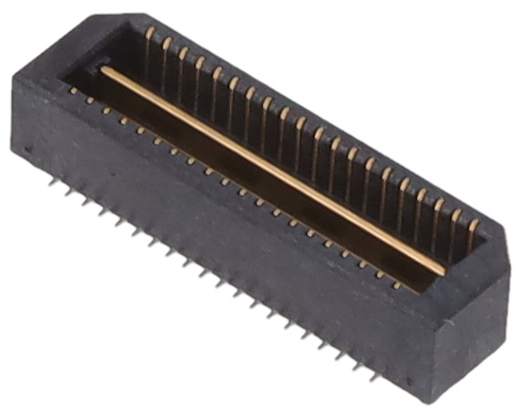
Part number: Samtec QTE-020-01-F-D-A
In the realm of RF systems, particularly mm-wave systems, there are also ganged coax connector products that can mount to a PCB and interface with a cable. For example, the ganged SMPM connector below.
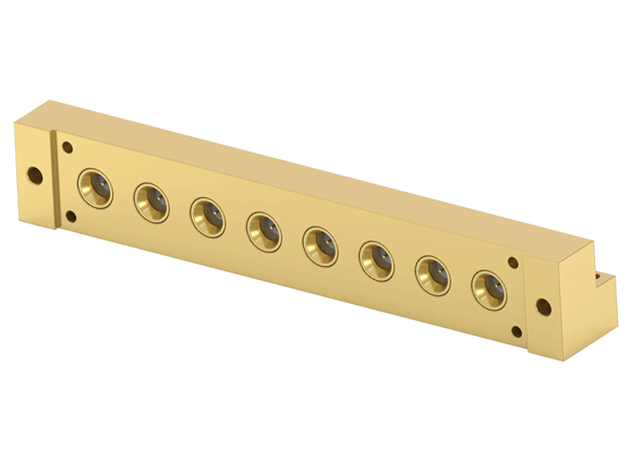
Part Number: TE Connectivity 2441485-1
Finally, I always like to present a through-hole connector example that can be found in VPX backplanes in order to illustrate the usefulness of these connectors, even in high-speed interconnects. While the connector does mount as a through-hole component, the board-to-board interface does not use pins such as you would find in a header. Instead, these are sliding contact connectors which are compatible with very high data rates.
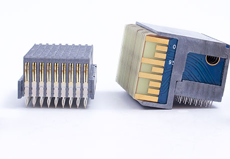
Amphenol SpaceVPX VITA 78 mating connectors
Because this particular connector is through-hole mounted into a circuit board, you would need to implement back drilling on the highest speed pins, or you would have to route across the entire stack-up. Another option is to use boomerang vias, but typically the boards in which this type of connector is used are not using HDI build-up layers due to concerns about reliability.
Therefore, if through-hole mount connectors are used to carry signals in high-speed digital channels, make sure to carefully plan routes so that you can route signals across the stack-up. This is where pinout planning will also become important, as we will see momentarily.
Pinout Design for High-Speed Multi-Board Interconnects
Pinouts for multi-board interconnects supporting high-speed signals need to include some ground reference across a board-to-board interconnect. This applies whether using direct board-to-board connections or board-to-cable connections. Just like in a PCB stack-up, where we allocate certain layers to ground planes, we would want to allocate certain pins to ground in a connector pinout.
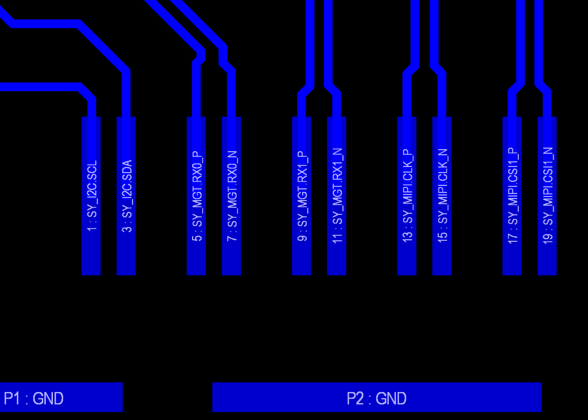
A very simple rule of thumb is to ground pins between digital signals. One of the common examples I show is in another article on routing in backplanes, specifically VPX backplanes. The image below shows differential pair routing into a pinout running at multiple gigabits per second. Note that this connector is a vertically mounted through-hole component, and the incoming traces are near the back layer to leave minimal leftover stub.

These Gbps differential pins are running diagonally in this pinout, and they are separated from each other by ground. Although you could get many more signals through this connector, allocating many of the pins to ground is essential for suppressing differential crosstalk and radiated emissions.
Pinout Guidelines
Follow these simple guidelines for pinout design to help ensure signal integrity:
- Use interleaved ground pins where possible
- Place single-ended pins adjacent to ground pins
- On differential pairs, place the positive and negative pins next to each other
- Avoid overlapping differential pins on multiple rows
- If there are unused pins, connect them all to GND
Why We Interleave Ground on Pins
In the above examples, you can see that the incoming signal pins are surrounded by ground pins. This is done for three reasons:
- To minimize pin-to-pin crosstalk
- To set a consistent input impedance into the connector
- To suppress radiated emissions from signals
- To contain common-mode noise on differential pins
These are the basic reasons we include ground pins on both single-ended interconnects and differential interconnects coming into a multi-pin connector. The main reason is to provide ground for single-ended signals, which will reduce radiated emissions and independent crosstalk, especially if a signal is routed out onto a cable. The second reason is that ground is often needed in cables in order to set the cable impedance, which is true for standardized cables with twisted pair cables, such as USB cables.
The same applies to connectors and cables with differential signals. While it is true that differential pairs are self-referencing, the presence of ground modifies the electric field around the differential pair, and that is why it impacts the potential for differential crosstalk.
Transmission Line Entry Routing
Signal integrity connectors for high-speed signals may not have any specific transmission line entry recommendations in the component data sheet when the traces are on the same layer as the connector pins. The connector will have some input impedance looking into your cable or mating connector, and that needs to be matched to the transmission line impedance. Normally, this is just a 50-ohm impedance for single-ended traces or a 100-ohm differential impedance for differential traces.
An important note on differential traces: a 100-ohm differential impedance, in this case, really corresponds to a 50-ohm odd-mode impedance. If the interconnect is differential, make sure you're matching the connector's differential impedance.
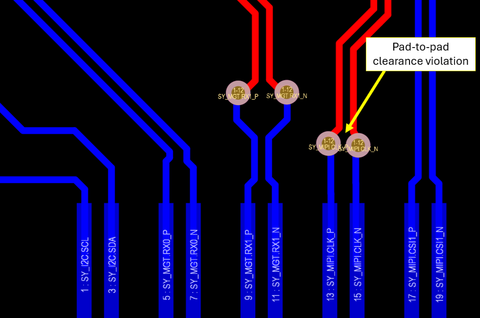
An example of line entry on a two-row high-density connector is found below. In the image, we have single-ended traces and differential traces.
In this trace entry image, the differential pairs far from the connector are spread out, but the traces come closer together during entry into the connector. It is appropriate to neck these closer together as the route comes into the connector pins, just like you might do if you're coming into the pins on an integrated circuit. The other notable feature of this connector is the central contact, which is allocated to GND, and it allows the usage of multiple differential pairs within the pin group.
Next, notice that the trace widths are similar to the pad size. It is possible to have the trace wider than the pad size, but you may need to neck down that trace coming into the pad. This may be required because as the traces come together near the pins, you might violate clearances, and neck down would be required. Remember, these are controlled impedance traces, so if you need to have narrower traces, you will need to make the substrate thinner or use a higher dielectric constant value.
Finally, we can have trace entry through vias, and this could be done as via in pad or a transition farther back from the connector pins. Depending on the pin pitch, you may need to space out the vias in order to prevent a clearance DRC error.
Remember that we are dealing with a connector rated for high-speed signals, so the via transition also needs to be intentionally designed. The intent is to match the via's characteristic impedance to the connector pin input impedance, with the end result being that the combined input impedance seen at the via matches your transmission line impedance. That means properly sizing the following:
- Antipad size
- Via diameter
- Via landing pad size
- Presence or removal of NFPs
- Location and number of stitching vias
This is generally the approach you would take when dealing with a single-ended or differential transition requiring high channel bandwidth. It starts to matter when you are working above approximately 3 GHz, which I have shown in detail in another article.
Analyzing High-Speed Links with Connectors Using S-Parameters
Just like other high-speed links, S-parameters can be used to analyze transmission lines with connectors and cables as part of the interconnect. Of course, it is possible to build an entire interconnect geometry using a 3D model of the connector body, and even a 3D model of the cable; you would then use a 3D electromagnetic field solver to determine the S-parameters for the entire link. Obviously, this is a very time-consuming task, which requires a lot of computing power as well as specialized software.
Thankfully, connector vendors who market their products for use in high-speed digital links or high-frequency RF links often provide S-parameter data for their products in Touchstone files. You can then use the connector vendor's data to create a linear network model for the interconnect and then determine the cascaded S-parameters.

Analysis tools like Simbeor, MATLAB, and Keysight ADS can then determine the cascaded S-parameters for this model. This then tells you the power transmission and losses along the entire interconnect. You can now predict how the link will function based on other parameters in your design that you can control, notably the transmission line design and connector entry design. In this network, the S-parameters for each individual section must be known, and then the simulator can calculate the cascaded network and its S-parameters.
What about the inverse problem, where you don't know the connector S-parameters? In this case, you would need to use measurements to de-embed the S-parameters for the connector. In this case, the connector forms the DUT in the linear network, and your connector S-parameters are determined from the cascaded network S-parameters using de-embedding. The same analysis programs listed above can also be used to de-embed the S-parameters for the connector as long as the S-parameters for the other components in the linear network are known.

About Author
Related Resources


Related Technical Documentation

Table of Contents
Get the Full Signal Analyzer Experience
- Turn SI analysis into fast, coordinated decisions.
- Your Agile Teams evaluation includes full access to Signal Analyzer.
Contact Us
Thank you, you are now subscribed to updates.

