Signal Integrity on Thin Ultra-HDI PCB Layers

To me it seems that every article about “advanced designs” focuses on faster edge rates, but it often leaves out the miniaturization. HDI designs bring PCBs to a solution space where signal integrity rules start to change due to the length scales involved in a typical design. One important class of materials has enabled HDI and UHDI designs with large numbers of high-speed interfaces: low-Dk PCB laminates. The story of HDI is linked to the story of low-Dk PCB materials, particularly once an HDI board implements a lot of high-speed digital interfaces.
Once you look at IC substrates and the typical materials used in these designs, you’ll find the same kinds of low-Dk materials that enable many high-speed digital designs, and perhaps this is where the PCB world got the idea for low-Dk PCB materials.
Newer HDI designs push the conventional HDI approach into overdrive, known better as ultra-HDI or UHDI. In these designs, the small copper features become a major factor limiting the channel bandwidth for high-speed interconnects, but low-Dk materials combined with smoother copper and innovative platings help overcome these problems.
In this short series of blogs, I will give an overview of how signal integrity relates to layer and feature sizes in HDI/UHDI PCBs, which we will see is closely related to high-bandwidth channels in packaging. To get started, we’ll review the manufacturability benefits of certain low-Dk materials.
Manufacturability With Low-Dk Materials
The first important point to note regarding the use of low-Dk materials is the manufacturability of HDI/UHDI feature sizes as a function of laminate Dk value. Take a look at the graph below to see what I mean.
For a given trace impedance target (say, 50 Ohms), the trace width will be fixed at some value that is a function of laminate thickness. When the laminate becomes too thin, the trace width requirement will be too thin, and the copper etching process will become more expensive, eventually switching to additive processing. The graph below summarizes this trend for low and high Dk values.

The counterpoint to this is the fact that not all low-Dk materials (such as Dk = 3 or slightly less) are available in very small film thicknesses required for UHDI PCBs or IC substrates. Low-Dk materials reaching down to a few mils with spread glass reinforcement are available with Dk values nearing 3 and approximately Df = 0.001. Examples are Megtron 8 and Tachyon 100G.
Note that this is thinner than an advanced PTFE laminate like Rogers 3003, but does operate in the same range of advanced PTFE with Dk = 3 or below with Df < 0.001. Rogers 3003, which I have used for outer HDI buildup layers in high-density radars, is currently only available as thin as 5 mils.
What Happens to Signal Integrity on Thin Layers
Based on the brief materials discussion I gave above, we can use this information to better understand the relationship between material properties, thickness of laminates, and signal integrity. We start with a few facts about the materials and geometry of traces in HDI/UHDI layers, especially when layer counts become high:
- Thinner layers force controlled impedance traces to be smaller
- Thinner layers generally bring ground planes closer to traces
- Device pinouts (e.g., fine-pitch BGAs) may force traces to be closer together
- Materials (copper and Dk value) can be used to tune signal integrity metric
When we get to UHDI devices, we might also decide to omit planes on certain layers, essentially creating skip-layer routing as is used in high-bandwidth digital channels in IC substrates. I’ll discuss this more below. First, let’s look at some of the important basic metrics, starting with losses and impedances.
Copper vs. Dielectric Losses
When operating in HDI and UHDI boards, the device pinouts and impedance requirements both require trace widths to be smaller, both for fanout routing from BGAs and controlled impedance routing. This could cause the dominant loss mechanism to switch from dielectric to copper when lower Dk is used.
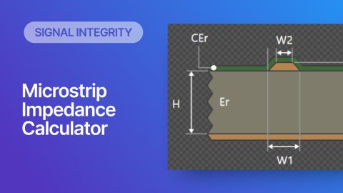
For example, take a look at the microstrip loss data below on a somewhat advanced FR4 laminate. The losses in the graph below are plotted as the voltage attenuation factor (see here for more details). The FR4 thickness is 38 microns (1.5 mil), the material data is (Dk = 4, Df = 0.01, thickness), and the layer uses 1 oz. copper with roughness of 1 micron. A 50 Ohm microstrip will be 57 microns wide.

Copper versus dielectric loss for a 57 micron wide 50 Ohm microstrip on FR4 (Dk = 4, Df = 0.01) and 1 micron copper roughness.
Now let’s suppose the laminate material is replaced with a sheet of Megtron 7(G) (Dk = 3.37, Df = 0.001) with the same thickness of 38 microns (1.5 mil). The 50 Ohm microstrip now requires a width of 68 microns. The greatly reduced dielectric loss now causes the copper loss to be the dominating factor up to very high frequencies.

Copper versus dielectric loss for a 65 micron wide 50 Ohm microstrip on Megtron 7(G) (Dk = 3.37, Df = 0.001) and 1 micron copper roughness.
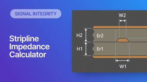
When we compare microstrips and striplines, we can see the loss penalty and linewidth values given the layer thickness requirements for a 50 Ohm single-ended line. I’ve included a hypothetical Dk = 2 material in HDI/UHDI thicknesses for comparison and to provide a theoretical limit. Similar results can be derived for differential lines.

We can clearly see a nonlinear divergence in loss for these single-ended traces once we get below approximately 2 mil layer thicknesses for all materials (Dk = 2 to approximately Dk = 3.5). This is due to the inverse relationship between skin effect resistance and trace width.
The takeaway: Using low-Dk helps with total losses in HDI/UHDI boards by forcing a wider trace width and reducing dielectric loss, but at some point the copper loss begins to dominate, and you get diminishing returns on your investment in laminate materials costs. Copper roughness reduction will be the only way to continue reducing total loss.
Plating Issues
Further reductions in conductor loss can be achieved by using alternative surface platings and smoother copper foils. For example, it is well-known that nickel-based platings can roughen copper at plating interfaces and create magnetic losses (such as in ENIG and ENEPIG platings). Research into more advanced platings is ongoing and plating issues are an active area of discussion for UHDI PCBs, both from the signal integrity aspect, as well as from the manufacturing (DFM/DFA) aspect.
To learn more about this issue with platings, watch our recent podcast episode with Kunal Shah.
Crosstalk Penalty
When taking a design with existing trace routing, and scaling it down to HDI/UHDI levels, the traces will come closer together and you would expect more crosstalk. At some point, the density of traces might require you to go below a conservative crosstalk rule of thumb, most commonly the “3W” rule. However, ground will be forced closer to the traces when layer counts are higher, and you would expect this to reduce crosstalk. Which effect wins out in a UHDI design?
The answer depends on a few factors:
- Are we using differential pairs and thus at risk of multi-mode crosstalk?
- Are we routing offset striplines or offset microstrips?
- Are we using high or low Dk laminates?
When scaling down to UHDI there could be a crosstalk penalty, meaning the crosstalk could increase as you pack traces closer together. Your job as a designer is to reduce the crosstalk penalty by adjusting the layer thickness and the Dk value. To better understand the effects of crosstalk, we need to use multi-port S-parameter simulations to better understand how crosstalk relates to laminate Dk value and laminate thickness.
The differential S-parameter spectra shown below illustrate the differences in crosstalk levels when switching from a Megtron 7 laminate (3 mil thickness, Dk = 3.37) to a Megtron 8 laminate (1.5 mil thickness, Dk = 3.06). These results were simulated in Simbeor on 100 Ohm symmetric differential striplines (trace-to-trace spacing = width) while varying the pair-to-pair spacing between 2W and 3W.

Differential symmetric stripline crosstalk spectra: blue curve shows NEXT, red curve shows FEXT.
As we can see in the above result, going to the thinner 1.5 mil Megtron 8 laminate with 3W spacing laminate increases the peak crosstalk to 4.38%. If we just switched from the 3 mil Megtron 7 to 1.5 mil Megtron 7 with all other parameters the same, the peak crosstalk would be 6.82%.
What is interesting here is that when we switch from 2W spacing on 3 mil Megtron 7 to 3W spacing on 1.5 mil Megtron 8, we see a smaller crosstalk penalty, as expected. One might assume that switching from 2W to 3W spacing gives a decrease in the routing density, but this is not the case. We still see a trace density increase of 108% by switching to the thinner Megtron 8 laminate, despite the smaller Dk. The return loss spectra for these interconnects show a bandwidth reduction of only 20% both for the 1.5 mil Megtron 7 laminate and the 1.5 mil Megtron 8 laminate.
The takeaway: In order to overcome crosstalk penalties with a given trace-to-trace (or pair-to-pair) spacing value (such as S = 2W), the spacing may need to be increased on the thinner laminate, and the dielectric constant may need to change. However, this does not always mean your trace routing density goes down. From the above example, we still have a doubling of the routing density, despite using a smaller Dk value. Very similar results can be derived for single-ended traces.
Fine-Line Routing of Differential Pairs
In UHDI routing into/out of fine-pitch BGA packages, the spacing between traces can be very small. This leads to very narrow traces that provide mutual ground references. This then creates some relaxation on the location of GND for a given layer. The reason is that each trace defines the impedance for the other traces; this is the same reason that differential pairs can function without being routed over a ground plane (this is not something you should do in every situation).
For example, fine-line routing with thicker layers would focus on the following type of differential pair design space:
- S ~ 1W to maintain differential impedance
- ~2 mil trace spacing
- S/H < 1 (thicker layers)
This approach forces you to increase trace density by reducing the value of S in order to maintain the target differential impedance value.
To really qualify what constitutes "too dense" in an HDI/UHDI PCB, the above simulations and analysis would need to be performed but with thicker PCB dielectric layers. This would give you the same kind of target crosstalk limit which can be enforced during routing as a PCB design rule.
Skip-Layer Routing and Offset Stripline Routing for High Bandwidths
Most UHDI PCBs and IC substrates will contain channels that are not extremely high bandwidth. Most pins will be for power, ground, configuration, GPIO, and slower serial interfaces. However, in processors with PCIe, DDR, multiple USB interfaces, and fast SerDes links, the routing in the substrate and PCB will be differential with a
Two very similar routing styles are available for differential pair routing in UHDI PCBs and IC substrates. These are:
- Skip-layer routing in IC substrates (not be confused with skip-layer vias)
- Offset stripline routing in HDI PCBs
These two are basically the same type of routing, but skip-layer routing uses a via fence to separate interconnects in a substrate. There are two reasons to use the via fencing in skip-layer routing: to provide shielding effectiveness against pair-to-pair crosstalk and to set the TEM-mode cutoff frequency beyond the receiving interface’s Nyquist frequency.

When we go to thinner dielectric layers with striplines (see above), we have a crosstalk penalty between these traces. However, with skip-layer routing, you could reduce the crosstalk penalty by adding the dielectric layer between the pairs as shown in the above arrangement.
If crosstalk between these signals is still problematic, crosstalk reduction could require any of the following to reduce the crosstalk:
- Increasing the via fence density
- Decreasing the via span across a channel (may increase channel bandwidth)
- Change the dielectric for different Dk
- Change the trace-to-trace spacing in the pair
In IC substrates and UHDI PCBs, any of these changes should be simulated and it can produce a decrease in crosstalk penalty, just like I show above in the crosstalk section. However, these changes could run up against manufacturing limitations, even in the case where a device is fabricated with an additive process. When the manufacturing limitations are being reached, the Dk value for the laminates may need to be changed.
Channel Bandwidth at High Speed
Not all interfaces on HDI/UHDI PCBs and substrates will require extremely high TEM bandwidth limits. But when they do, there could be a channel bandwidth penalty when switching to a thinner layer. This could result from increased copper losses, which creates an impedance deviation from the interconnect’s target value at higher frequencies due to the skin effect.
However, depending on the laminate’s Dk value, the load, and the type of channel, any channel bandwidth limitation could occur at such high frequency as to be negligible, or there could be a channel bandwidth increase. This is not so important in interfaces like MIPI or USB, but it matters greatly in DDR4/5/6, PCIe 5.0 or higher, and 25G or faster Ethernet. Studying channel bandwidth requires looking at TEM bandwidth limits in coplanar waveguides, such as in RF boards, something which I plan to present in more detail in the future.
Whether you need to build reliable power electronics or advanced digital systems, use the complete set of PCB design features and world-class CAD tools in Altium Designer®. To implement collaboration in today’s cross-disciplinary environment, innovative companies are using the Altium 365™ to easily share design data and put projects into manufacturing.
We have only scratched the surface of what’s possible with Altium Designer on Altium 365. Start your free trial of Altium Designer + Altium 365 today.


