How to Design High-Speed & RF Via Transitions
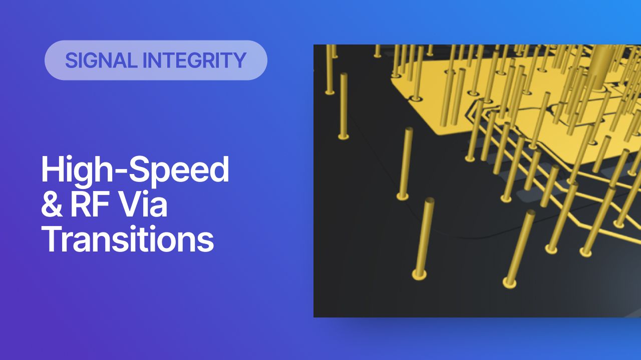
There is sometimes a design guideline seen in high-speed PCB design stating that vias should be avoided on signal traces, both for single-ended signals and differential pairs. This is not totally incorrect, but it does require a bit of context. When signal bandwidths are very broad, reaching well into the GHz range, the via transition must be carefully designed to provide low return loss at the input of the via. In addition, once considering the routing into/out of the via, the placement of the via should not modify the insertion loss of the equivalent channel without the via.
In this article, I’ll outline some of the main concepts required to understand how to design these via transitions so that signals can be routed between layers in a PCB. Via transitions are about designing to impedance, as well as ensuring manufacturability for the via structure you create. The concepts outlined here should help you understand how to work with more advanced design tools to build layer transitions with stitching vias.
Via Transition Manufacturing, Antipads, and Stitching Vias
I think the first place to start when designing a via transition is to understand the structure that you need to manufacture. The primary tool used to correctly design layer transitions for high-speed vias and RF vias is stitching vias. The design of an RF/high-speed via transition requires precisely placing stitching vias around a signal via such that the
- Via size - The via drill diameter will always be limited by the fabrication house’s drilling capabilities. There is no strict requirement on the via size required for a specific signal or frequency.
- Antipad size - In high-speed design and in RF PCB design, the via transition will need to pass through at least one plane layer, and the antipad in the plane needs to be sized correctly as it helps determine the impedance.
- Spacing between vias - There will be some limit to the wall-to-wall spacing between the vias that can be fabricated.
- Pad size - The limit on the pad size will determine . Also, note the annular ring requirements in Class 2 or Class 3 products.
- Backdrilling - The discussion below will not consider backdrilling specifically, but it helps to determine whether you will make a layer transition that requires backdrilling. Learn more about determining backdrilling needs here.
- High density vs. standard fabrication - Will you be using HDI buildup for your board, and you need backdrilling? If so, consider using a high-density approach with blind/buried vias for your layer transitions.

To get started designing a via transition between two layers, make sure you determine the answers to these questions first. The first two are most important because they relate to the DFM requirements for your board, and this will then limit the frequency (or bandwidth) you can reliably transfer across a via transition.
How to Design Via Transitions
All via transitions are about designing the via impedance to have the required value within your required signal bandwidth. This is done by sizing the following physical aspects of your board:
- Number of stitching vias
- Arrangement of stitching vias
- Pad size and antipad size
- Inclusion or removal of NFPs
Some of the main signal integrity goals for these via transition designs are shown in the table below. Note that I’ve mentioned that insertion loss is an important factor. Generally, insertion loss is just not the primary design goal for the via structure, but the interplay between the routing into/out of the via structure and the design of the via structure itself can create a strong increase in insertion loss that limits the bandwidth of the entire channel.
|
|
|
|
|
|
|
|
|
|
|
|
|
|
|
|
|
|
|
|
Unfortunately, there is no analytical set of equations to this problem that is generalizable to any layer count or stitching via structure. The geometry and boundary conditions just make the problem too complex such that it is analytically intractable. Also, due to the cylindrical geometry of via arrays, the problem involves relations with cylindrical Bessel and Neumann functions, and I’m sure no engineer wants to spend their time deriving these relations by hand.
Therefore, we have to use some conceptual tools to set the stitching via spacing around the signal via (or pair of vias for a differential channel). Let’s look at a few cases:
Below 3 GHz: Worry About Return Path
Below about 3 GHz, the input impedance of the via transition typically will deviate significantly from 50 Ohms as long as there is a nearby ground return via. Therefore, unless you’re operating with very fast channels, don’t worry about placing a specific stitching via structure into/out of a via transition. A typical antipad size will be at least as large as the landing pad size. As long as there is a return via somewhere nearby, you will maintain a sufficiently tight current loop to reduce EMI/susceptibility. I’ve discussed this in my other article on stitching vias.

The reason for this is that the input impedance is what matters, and the input impedance at the via transition will look like the trace impedance (i.e., the via is electrically short). The same applies to differential pairs. The via transitions start to really matter above 5 GHz.
Above 3-5 GHz
I’ve stated (and shown with calculations/simulations) many times that the via impedance does not matter until signal bandwidths exceed 3 to 5 GHz. If you just have a via transition with no stitching vias, the impedance of the transition will look inductive and will increase up to about 3-4x the via transition’s characteristic impedance until about 30 GHz. Above that frequency range, the capacitance takes over, and the via impedance starts to drop again until ~50 GHz.
Placing some stitching vias as shown below and reducing the antipad size will reduce the impedance rise from the 5 to 50 GHz range. This is because the vias and antipad determine the capacitance seen in parallel to the signal vias, which reduces the via’s characteristic impedance and thus the input impedance. When the vias and antipad boundary are moved closer, the impedance decrease will be greater and will get closer to the impedance target (either single-ended or differential).

For differential pairs, the antipad will dominate the effects on input impedance, while single-ended channels have similar sensitivity to both antipad size and via arrangement.
If you bring the vias and/or antipad too close, you’ve added too much capacitance, and then the input impedance will dip below your target in the 5-50 GHz range. With just the right arrangement of vias, you can hit your target impedance and maintain nearly flat input impedance up to 40-50 GHz, which is sufficient for very fast 112G PAM-4 signaling.
I mentioned above that there are no analytical solutions to the via transition design problem, so there are no closed form models that will work in the frequency ranges where via impedance actually matters. This is the reason that every via impedance calculator I have seen produces incorrect results and is not useful in real situations. I’ve discussed this problem in another article; this is also why you will need some application like CST or Simbeor to design interconnects with flat impedance within the desired signal bandwidth.
Is There a Through-hole Via Transition Maximum Frequency?
What kind of maximum bandwidth can you expect in these designs? The value will be somewhere below ~100 GHz for RF signals, and flat impedance can be designed up to ~50 GHz for digital signals.
The main factor that limits the bandwidth/frequency you can pass through a via transition is the fabrication technology used to build the via transition. This is because the drill size and stitching via spacing will be limited. In order to build layer transitions beyond ~90 GHz, we need a different fabrication technology.
With that being said, the limits in current subtractive etching and drilling fabrication technology still enable through-hole via transitions operating well into mmWave bands. At my company, we’ve designed via transitions at 77 GHz for radar designs. At these frequencies, most designs focus on the use of a blind via to make a layer transition, but through-holes are actually very important in areas like dense hybrid beamformed MIMO radars and in 5G antenna arrays operating in mmWave bands. I’ve shown this in my recent EDICON presentation.

The risk here is that there could be excessive leakage of the signal from the via array, which is indicated by the localization frequency limit (in green).
The RF world has done a lot of work to create precise layer transition designs that can operate well into the GHz range that are not based on through-hole vias. These have helped get past the ~90 GHz limit found in wideband connector lands from BGA components and the types of narrowband transitions shown above. Some of the alternative types of signal transitions that can span part or all of a PCB layer stack into the mmWave range include aperture coupling and stepped blind/buried via coupling.
Unfortunately, these are all narrowband, meaning you cannot get a high-speed signal through these via transitions. You will start to lose power in midrange frequencies, something which can be clearly seen in return loss measurements at the signal transition. I’ve done via transition designs for differential SerDes channels that very clearly provide enough bandwidth for a through-hole transition that can support 56 GHz bandwidths (this is the Nyquist frequency for 224 Gbps PAM-4 bitstreams) on Megtron substrates.
In the designs I’ve done in these areas, we have no choice but to use through-holes because we have patches packed on one surface layer, with transceivers packed on the other surface layer. However, to design and specify these transitions, you need an electromagnetic field solver, a clear fabrication drawing, and of course you will need the industry’s best CAD tools.
Summary
In summary, I’ve developed the following table that lists when a stitching via array is needed, when only a single return via is needed, and when no vias are needed for signal transitions across multiple layers.
|
|
|
|
|
|
|
|
|
|
|
|
When you’re ready to create a PCB stackup and layout that supports high speed/high frequency layer transitions through vias, use the complete set of product design tools in Altium. The CAD features in Altium enable all aspects of systems and product design, ranging from packaging and PCB layout, and up to harness and cable design. When you’ve finished your design, and you want to release files to your manufacturer, Altium makes it easy to collaborate and share your projects.


