The Basics of Signal Integrity Analysis and Simulation in PCB Design

At a Glance
Read and learn the important steps in signal integrity analysis and how these steps reveal problems in your PCB layout.


The basics of signal integrity analysis in your PCB design can be anything but basic. Signal integrity simulation tools are great for calculating the behavior of signals in different nets during schematic and layout design, but you’ll still need to take some steps to interpret the results. As advanced as some signal integrity and EM simulation tools can get, they simply can’t compare to the information you can glean from measurements. Whichever method you use to examine signal integrity in your board (you should do both), there are some important steps you can take to analyze the behavior of your signals and identify problems in your board.
Getting Started with Signal Integrity Simulation and Analysis
Signal integrity analysis begins with simulations at the pre-layout phase. Once you build up your layout, you can use some important post-layout simulations to analyze geometry-dependent signal integrity in your board. At some point, you will need to compare your signal integrity simulation results with real measurements, so keep your results handy for comparison.
Pre-Layout Signal Integrity Analyses
This portion is really about circuit design, component selection, and examining how signals travel between I/Os on two components. There are three important analyses that tell you a significant amount of information about your board’s behavior.
-
Transient behavior. Transient responses in the connection between two buffers can also be modeled in the time domain using transient analysis, or you can determine the behavior of transients from pole-zero analysis. This will show you overshoot/undershoot due to ringing and the approach to the intended signal level. The most accurate versions of these signal integrity simulations with integrated circuits involve IBIS models, although SPICE subcircuits could be used to model I/O buffers.
-
S-parameters and transfer function. Certain functional blocks in your board can be modelled as multiport networks, meaning their linear behavior can be described in terms of S-parameters at a particular frequency. You can determine the S-parameters from a reflection coefficient in the time domain, which in transmission lines involves the input impedance given by the load capacitance. You can calculate the transfer function for your network from the S-parameters, and vice versa. Here’s an excellent guide that shows all the mathematics involved.
-
Impulse response. This signal integrity simulation involves two goals: qualifying S-parameter models/transfer function for causality in your defined bandwidth, and examining the pulse response behavior for a defined rise time. Impulse responses also allow you to extract dispersion and propagation delat along your interconnect design. This qualifies an intended channel model for a given input/output buffer pair in an ideal situation before you layout the PCB design.
-
Eye diagram. Buffer models and the interconnect design can be used to simulate an eye diagram. The eye diagram is an important part of channel compliance as it will show expected signal level, overshoot, intersymbol interference (ISI), jitter, and expected bit error rate under a pseudorandom bit sequence.
In more complex channels, the above set of pre-layout analyses can help you qualify things like planned via transitions,
As long as you know the structure of each of these elements before you create the design, you can
Post-Layout Analyses
This portion is really about examining how parasitics in your board affect signal integrity. As parasitic signal integrity effects are functions of board geometry, you’ll need to examine the following geometry-dependent signal integrity problems:
-
Crosstalk. The bane of many designers, crosstalk arises from inductive and capacitive coupling. If you are examining the effects of crosstalk on a victim and aggressor trace, capacitive coupling will only occur when the two are adjacent. Inductive crosstalk is not limited by range, and all traces in your board can couple to each other via the magnetic field.
-
Transmission line behavior. While you can use transmission line models to examine signal traces during the pre-layout phase, it is best to do this directly from your layout. If your lines are not impedance-controlled, then you will need to examine whether reflections on the line (if any) degrade signal levels at the receiver and lead to a stair-step response with digital signals. With analog signals, this can be more tricky, as you are looking for interference and standing wave formation on the line. However, the right signal integrity simulator can separate the incident and reflected waves, allowing you to examine the behavior of each individually. You can then determine the level of reflection and see if the signal level meets your signaling requirements.
-
Everything you examined pre-layout! The point here is to check that parasitics, fiber weave, etc. do not dramatically alter the behavior of signals in your board. If multiple traces are failing, then your layout will need to be modified. The first place to start is with your stackup and trace geometry.
Signal Integrity Analysis Tools
The above points might as if you need a complex simulator program to build and run these signal integrity analysis tools. The exact tools you need will depend on what you want to simulate and evaluate. Inside your EDA tool, some of these signal integrity simulations are simply done with something like IBIS, while more complex simulations with multiple nets can require a 3D field solver or a comparable 2D solver tool.
Single-ended Buses With No Impedance Spec
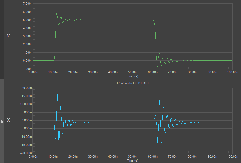
In slower single-ended buses without termination, it is possible to observe some transient behavior (ringing) that could be due to the structure of the interconnect (its capacitance and inductance). This is something that could be observed in SPI when the trace is electrically short. In these buses, it is possible to observe ringing pre-layout as long as you have a transmission line model applied in your schematics and as long as the pin specification is defined (either SPICE subcircuit or IBIS model).

When the single-ended bus is actually routed, you can run a post-layout simulation with the signal integrity analyzer in your EDA tools. These analyzers can use either a logic family assignment or an IBIS model for the relevant pins/nets to simulate:
- Crosstalk waveforms, and to identify strong coupling regions
- Reflection waveforms
- Other signal behavior metrics (rise/fall time, overshoot/undershoot, etc.)
- Calculate average impedance along the length of the track
In single-ended buses without an impedance specification, it is possible to observe reflections at the driver end when the bus gets long, or ringing due to the capacitance and inductance on the bus. If ringing produces excessive overshoot, then reducing the trace inductance and adding damping are the two main paths forward in reducing the ringing amplitude. The other is to increase damping by adding a series resistor, something which you would do with a low-impedance buffer output into a longer mismatched transmission line.
Impedance Controlled Buses
In single-ended and differential impedance-controlled buses, the terminating impedance could be on-die, so a logic family-based simulation in post-layout is not effective as it does not correctly describe the impedance of the bus. Crosstalk can still be simulated because you are only looking at coupling between two interconnects as a function of rise time, and the crosstalk magnitude will inversely scale with rise time accordingly, even if you only assign a logic family.
In the case of a post-layout simulation for reflections and impedance violations, a signal integrity simulation in this case should at least use IBIS models to define buffer behavior rather than relying on logic family descriptions. As long as the buffer description is known and available, it can be applied to model the behavior of the component in the PCB Editor. Standard signal integrity tools in a PCB editor for crosstalk and reflection waveforms can help with a lot of up-front qualification of signal behavior (rise/fall time, overshoot, crosstalk, consistent impedance, and ringing) before moving into a more advanced signal integrity analysis tool.
To simulate things like eye diagrams, multi-net crosstalk, and impedance deviations along the length of a net, there are external signal integrity analysis tools that can be used. Field solvers are one option, and there are many of these tools available with different levels of specialization. Something like a full-wave field solver is not always necessary unless you want to simulate radiated emissions, something deeper with SI/PI, or extract S-parameters in the simulated net.
The powerful PCB design and signal integrity analysis tools in Altium Develop give you a useful starting point for signal integrity analysis with pre-layout and post-layout signal integrity simulation tools. These accurate calculations give you a baseline for comparing your measurements. You’ll also have access to a complete set of manufacturing planning and documentation features in a single platform.

About Author
Related Resources


Related Technical Documentation

Table of Contents
Get the Full Signal Analyzer Experience
- Turn SI analysis into fast, coordinated decisions.
- Your Agile Teams evaluation includes full access to Signal Analyzer.
Contact Us
Thank you, you are now subscribed to updates.

