Routing Differential Microstrip Traces with Controlled Impedance


Modern digital systems and low-level analog boards need methods for achieving precise characteristic impedance calculations and impedance control. Differential microstrip and stripline pairs have common-mode noise immunity if they are routed symmetrically, but they also need to have controlled differential impedance to ensure impedance matching and consistent propagation delay throughout an interconnect. With the differential microstrip impedance calculator in Altium Designer, you’ll have the design features you need to determine the best surface trace geometry to ensure consistent impedance in your PCB.
ALTIUM DESIGNER
High-speed designs often use differential pairs for signal routing. This simple concept provides digital systems with high common-mode noise suppression, which encompasses nearly all noise sources in your PCB. In order to use differential pairs properly, including differential microstrip traces and striplines, their width and spacing needs to be carefully chosen to ensure they have consistent differential impedance.
While there are some formulas you can use to calculate differential impedance from geometry, reversing the process and calculating the geometry from differential impedance is difficult. Differential impedance is also related to the propagation delay along a trace, and this quantity must be known to ensure length matching between each signal. Altium Designer now includes an integrated electromagnetic field solver that calculates your differential pair impedance automatically and allows you to focus on designing the best PCB layout. The routing tools also help you layout your board with accurate routing and skew compensation in your interconnects.
Differential Microstrip Traces Require Controlled Impedance
Coming up with the correct trace widths and spacing between the pairs is important when controlling the impedance, and calculating those values is the key to success. There are many calculators available online, as well as built into your PCB design software. Controlled differential impedance starts with characteristic impedance. The characteristic impedance of your microstrips is determined by the trace width for a given layer stackup.
Once you know the characteristic impedance, the differential impedance is determined by setting the spacing between each side of the differential pair. By setting the right spacing between your microstrip traces, you’ll set the differential microstrip impedance to a specific value. Some empirical formulas have been determined in the past, but the most accurate results for both types of impedance are obtained when you have access to a differential microstrip impedance calculator in your PCB design software.
Altium Designer Provides the Right Set of Tools for Controlling Impedance
Before you start routing those differential microstrip traces on your board, you should find a reliable differential impedance calculator. The integrated electromagnetic field solver in Altium Designer provides accurate differential impedance calculations for microstrips directly from your PCB stackup. You won’t need to manually enter layer thickness values or calculate the dielectric constant of your substrate at your operating frequency; everything is done for you in Altium Designer.
- Determining differential microstrip impedance starts with determining the characteristic impedance for your microstrips.
Learn about determining characteristic impedance in microstrip traces.
- Your layer stack determines dielectric thickness and ground plane distance, which then sets the effective dielectric constant seen by signals. These factors then determine characteristic and differential microstrip impedance.
- Although you need an accurate calculation of differential microstrip impedance, you can get a quick estimate using some simple methods.
Learn about some methods for estimating differential microstrip impedance.

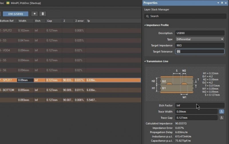
Altium Designer’s enhanced layer stack manager will calculate impedance profiles for your differential pairs.
Differential Microstrip Propagation Delay and Skew
Coming up with the correct trace widths and spacing between the pairs is important when controlling the impedance, and calculating those values is the key to success. Differential pair routing establishes a balanced transmission system that carries the equal and opposite differential signals across the PCB. The objective in PCB routing for differential signals is to ensure that the pair of signals arrive at the target at the same time.
The time required for signals to reach the end of a differential pair is determined by the differential impedance, which is related to the propagation delay. The signal speed in a stripline is simple; it’s just determined by the dielectric constant of the substrate. In a differential microstrip, the signal velocity depends on an effective dielectric constant, which then depends on the geometry of the differential microstrip pair. Accurately determining the propagation delay in a differential microstrip takes an integrated field solver in your PCB routing tools.
Using Differential Microstrip Propagation Delay Calculations in Your PCB
Altium Designer has automatic functions that speed and simply differential microstrip propagation delay calculations. The unified design environment provided by Altium Designer eliminates the need for shifting out of the design, loading a third-party calculator, and manually feeding the calculations back into the design.
By determining the propagation delay for your differential microstrip traces, you can reduce skew between each signal in a differential pair and ensure your signals arrive at the receiver on time. By setting your allowed skew as design rules, the routing tools in Altium Designer will check each end of the differential microstrip pair against your design tolerances. Altium Designer’s integrated differential microstrip impedance calculator automatically determines skew from the board layer stackup and routing geometry as you create your PCB layout.
- Skew compensation in your board is about more than tuning trace lengths. You can use delay/phase tuning for breakouts to keep differential pairs properly coupled and length matched.
Learn more about delay tuning for differential microstrip traces.
- Your propagation delay results will be immediately imported into your differential pair routing features as you create your PCB layout when you use Altium Designer.
Learn more about length tuning for differential pairs in Altium Designer.
- The integrated field solver in Altium Designer also helps you analyze crosstalk between microstrip and stripline traces in your PCB.

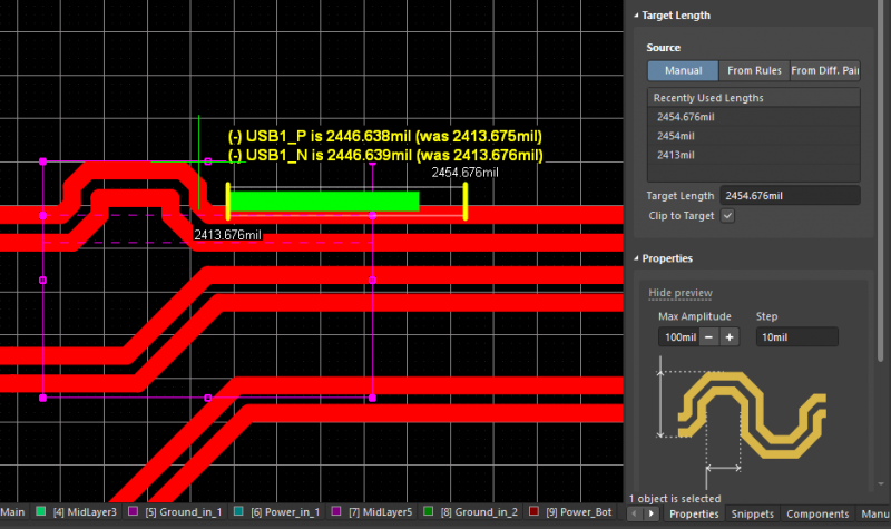
The length tuning interface for differential microstrip pairs in Altium Designer.
Try the High-Speed Routing Tools in Altium Designer
The differential pair routing tools in Altium Designer let you push, shove, and gloss your differential microstrip, stripline, and coplanar waveguide traces while maintaining their desired width and spacing rules. Altium Designer goes even further than that with an advanced set of high-speed rules to control measured lines, signal paths, routing topologies, and much more.
Intuitive user control allows you to add length tuning segments by wiping the cursor along the route path. Altium Designer relies on a length tuning algorithm to automatically calculate the dimensions and positions of the tracks and arcs used for building the tuning segments. You can base the properties used for length tuning on design rules, properties of the net, or specified values.
Improve Your High-Speed Routing with Altium Designer
From schematic capture to PCB layout, Altium Designer includes everything you need to create your next PCB. The rules-driven design engine helps you evaluate your board as you create your layout, including your differential microstrip pair impedance and propagation delay tolerances. No other system provides this many powerful features in a single program.
- Only Altium Designer includes the design features you need to create schematics, PCB layouts, and manufacturing documentation in a single program.
Learn more about the unified design environment in Altium Designer.
- The integrated 3D electromagnetic field solver automatically determines dielectric constant, including a model for dispersion and dissipation. You’ll have the features you need for accurate impedance calculations.
Learn more about Simberian’s integrated field solver in Altium Designer.
- Creating the final manufacturing documentation for your design has never been easier with Altium Designer’s Draftsman and ActiveBOM tools.
Learn More about Altium Designer’s Draftsman to create your design’s documentation.

Find your high-speed PCB design solutions in Altium Designer.
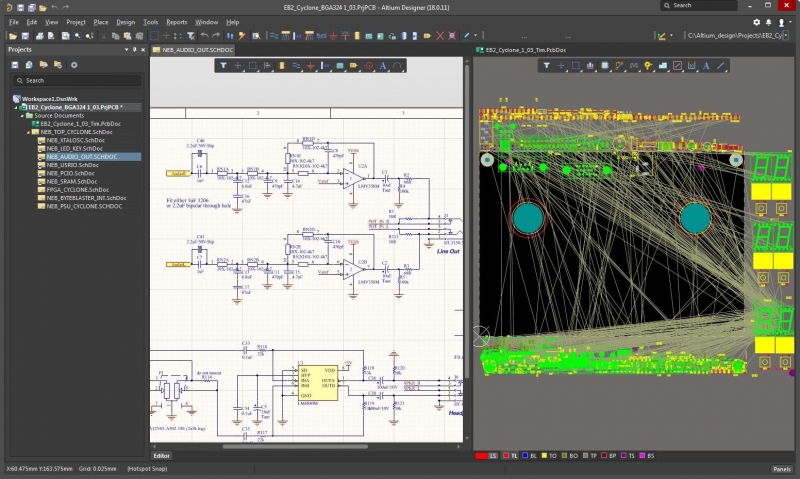
The schematic editor in Altium Designer makes it easy to define differential pairs and set electrical design rules. From there, you can move the differential pair definitions to the PCB with design synchronization, transfer the differential pairs to the PCB editor, and then view and manage differential pairs on the PCB. Altium Designer’s unified environment makes it easy to create any schematic, route traces, create a PCB layout, and output the final manufacturing documentation.
Altium Designer on Altium 365 delivers an unprecedented amount of integration to the electronics industry until now relegated to the world of software development, allowing designers to work from home and reach unprecedented levels of efficiency.
We have only scratched the surface of what is possible to do with Altium Designer on Altium 365. You can check the product page for a more in-depth feature description or one of the On-Demand Webinars.


