Gerber Compare in Altium 365's Online Platform

The moment you push your Gerbers to a manufacturer for a DFM inspection, it can be a nerve-wracking experience waiting for a response. Once I push a totally new design to manufacturing, I spend a few sleepless nights waiting for a pro forma quote to come through and the design to pass qualification. It’s not until I get working boards that I breathe a sigh of relief. But before you receive your working boards, there will likely be some back-and-forth communication before your board hits the fabrication line.
When manufacturers and designers need to resolve problems in Gerber files before fabrication, it helps to have a Gerber compare utility. The newest version of Altium Designer now offers this feature through the Altium 365 platform, giving everyone visibility into changes to Gerbers before fabrication. This helps designers get to market faster, increases throughput for fabricators, and keeps everyone informed during the fabrication process.
What PCB Manufacturers Look For in Your Gerber Files
The extent to which a PCB manufacturer will review and modify your Gerber files depends on the level of service you need for your design. In full turnkey services, you’ll likely get a complete inspection, sourcing services, complete manufacturability and assembly review, in-circuit testing, and
During a design review, your fabricator may look through your project files and your Gerber files to spot any problems that compromise board quality or yield:
- Standards conformance: Your design might need IPC Class 2, Class 3, 6012, or other inspection level. Fabricators will start looking for reliability defects in your Gerbers to ensure you’re compliant with your standards level and to ensure fabrication quality.
- Footprint mismatches: PCB land pattern/footprint mismatches or other problems with footprints that impact assembly can be noticed in Gerber files.
- Drill hits: Overlapping drill hits, drill hits into pads, or mis-sized drill hits can be spotted in Gerber files and a drill table.
- Clearances and feature sizes: Clearances between pads (smallest component pitch), between traces, and smallest feature sizes in general will determine some fabrication costs and potential for fabrication/assembly defects.
In some cases, the Gerbers are simply outdated and need to be regenerated. In other cases, they may need to be manually modified and submitted back to the customer for review. Whenever files need to be regenerated or modified, the fabricator needs to get approval from the customer on the finalized files before starting a production run.
No matter who regenerates Gerber files and other manufacturing documents, it helps for the designer and fabricator to be able to compare each version of a file side-by-side to ensure all outstanding issues have been addressed. I’ve had fabricators send me Word documents with current and modified files for comparison, which I then had to comment on and send back. It’s easy to have text be misinterpreted, images be unclear, or files to get corrupted. Altium Designer and Altium 365 solve this problem with integrated Gerber viewer and Gerber compare features.
Save Time With an Online Gerber Compare Tool
All of these factors waste time on back-and-forth clarifications when the fabricator could be getting the board into production. Thankfully, Altium 365 now includes a Gerber compare feature that lets everyone involved in a project see different versions of Gerber files side-by-side. Because Altium 365 functions as a version control service based on Git, Gerber files that are part of version control can be accessed, modified, and compared within Altium Designer.
To take advantage of this feature, you need to work with Project Releases within Altium Designer. The goal of a Project Release is to prepare a complete package for fabrication and assembly that includes all relevant fabrication files, including Gerber files.

Once two Project Releases are present in your managed content server, and both releases include a complete set of Gerber files, you can access the Gerber compare feature. Similarly, when Project Releases are sent to a manufacturer, the manufacturer can open each release and compare the Gerber files from these releases.
Gerber Compare Example
Altium Designer already includes built-in file comparison features, and users can even compare Gerber files stored on their local machines. You can even download releases from a project, import Gerber files, manually, and set up a file compare in Altium Designer. Now Altium 365 allows users to compare Gerber files from successive project releases in their web browser without opening these files in Altium Designer. This is a simple way to access and compare Gerber files from multiple project releases from anywhere in a secure web platform.
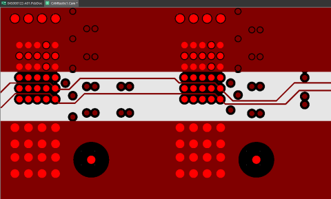
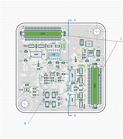
The image below shows one example of a Gerber comparison in Altium 365. The specific features that were modified between releases are highlighted in red. General areas in each layer are also marked for easy identification and inspection. This is a simple way for manufacturers and their customers to get a design through review and qualify any required changes before fabrication.

With a bit of layer manipulation, you can focus on the specific portions of the files that are different, both from the above comparison map and by flashing between the two compared layers. As another example, the image below shows a Gerber compare where some tracks were removed (shown in green) while some tracks and polygons were added (shown in red). This alternative view is a quick way to run a Gerber compare directly in fabrication files without downloading project releases.

Comparisons can be run for any pair of Gerber layers in the project release files. After looking at this type of comparison, a manufacturer can call out specific portions of the design in comments to ensure the designer will make changes before fabrication.
Since all files in a Project Release are stored on Altium 365, files from old revisions can still be accessed and downloaded directly. A manufacturer can also instantly open the new project release in Altium Designer and identify variations between two design documents using the Differences panel. Comments can also be left in the most current version to ensure they are seen and addressed by the design time. Once changes are made, a new Project Release can be pushed back to the manufacturer for a final review before production.
Today’s PCB manufacturers and PCB designers can work together to get through production quickly, reduce defects, and streamline sourcing thanks to the Altium 365™ platform. This unique cloud-based platform integrates with the world-class design tools in Altium Designer®, making all your project data accessible to your manufacturer and collaborators in a secure environment. Designers and manufacturers can share PCB fabrication data, project files, and much more in a cloud-based platform.
We have only scratched the surface of what is possible to do with Altium Designer on Altium 365. You can check the product page for a more in-depth feature description or one of the On-Demand Webinars.


