


Simple Documentation for Hand PCB Assembly

At a Glance
Sometimes you might take a product or a prototype in-house to assemble. Here's how to prepare for hand PCB assembly.


Whenever we talk about PCB assembly, we always bring up the automated route, involving pick and place machines and automated soldering processes. Even though hand assembly is not often done at scale, it's still quite common in low volume production, prototype PCB assembly, and PCB rework. You can ensure your assembly will be error-free if you use some simple documentation practices that will aid assembly technicians.
Preparing hand PCB assembly documentation does not preclude the same documentation from being used to aid automated PCB assembly. So if you want to streamline your hand PCB assembly and overall assembly processes, here is what your data should look like.
What PCB Assembly Technicians Need
PCB assembly technicians will need a few pieces of documentation that are mandatory for streamlined assembly. If you get this documentation correct, you will avoid some simple errors that could make your design non-functional.
The main document your assembly technician will need is an assembly drawing. The drawing needs to be very clear and have a few important pieces of information on it. In most cases, your assembler will not have the actual design open in front of them, and most assembly technicians do not work in CAD tools anyway. You will instead need to make sure a clear assembly drawing includes the following:
-
A realistic 2D drawing or 3D view with component outlines
-
An assembly layer rendering, preferably with mask openings to show component leads
-
Polarity markers, pin 1 markers, and reference designators in the assembly layer rendering
-
Assembly notes that specify soldering requirements
-
Board-to-wire connector pinouts for hand-assembled cables
-
Parts kit with each unique part marked with reference designators
-
2D or 3D views with component outlines
A 2D or 3D view with component outlines will not be used as the primary guidance for assembly, but it is quite useful as a way to verify that the major parts are in the right locations. In many CAD tools, you would have to create this by manually exporting component outlines to a DXF file or creating a 2D projection from a 3D STEP file in MCAD software, and then this would be used in drafting software to create an assembly layer rendering.
In Draftsman, you can create this view automatically, see the example output below.
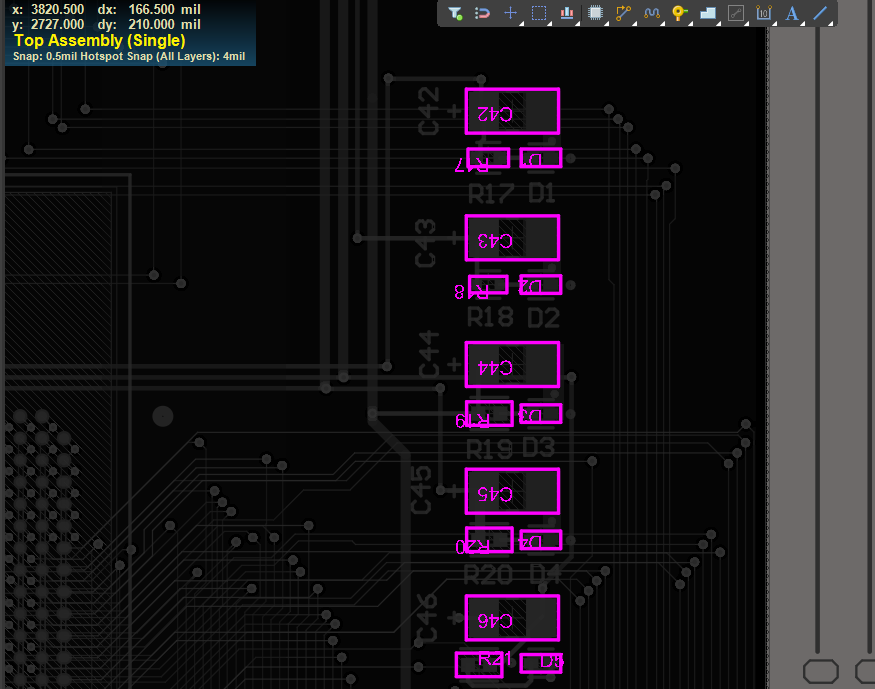
Assembly Layer Rendering
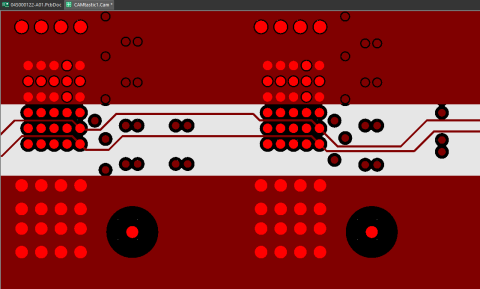
An assembly layer rendering will be the main document that guides assembly. It is also quite helpful if the PCB has reference designators shown on the surface layers.
An assembly layer rendering should show component outlines and lead locations in a single drawing. This can be created by overlaying an assembly layer and paste mask layer. By creating this overlay, it very clearly shows the solder and lead locations around each component in a single view, as well as the reference designator for each component.
If you are going to use an assembly layer to create the rendering, make sure the reference designators in the assembly layer have been cleaned up and are clearly visible around each part. See below for a bad example of an assembly layer.
Don’t let your assembly layer look like this
The other important thing to include in this assembly layer rendering is pin one designators, a diode symbol, or other polarity indicators for ICs and polarized components. Other components like passives that are unpolarized or rotation-proof do not require these markings.
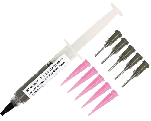
Soldering Requirements
Soldering could involve the application of solder paste through a stencil or manual soldering with a wire. In either case, make sure the required solder composition is specified if there is a requirement. For example, if your hand-assembled PCB is to be lead-free processed, then make sure to specify a lead-free solder wire or paste to be used in the design. This can be done in the assembly notes.
Specify solder material requirements in your notes. At minimum, specify if soldering must be RoHS compliant
Connector Pinouts and Wiring Diagrams
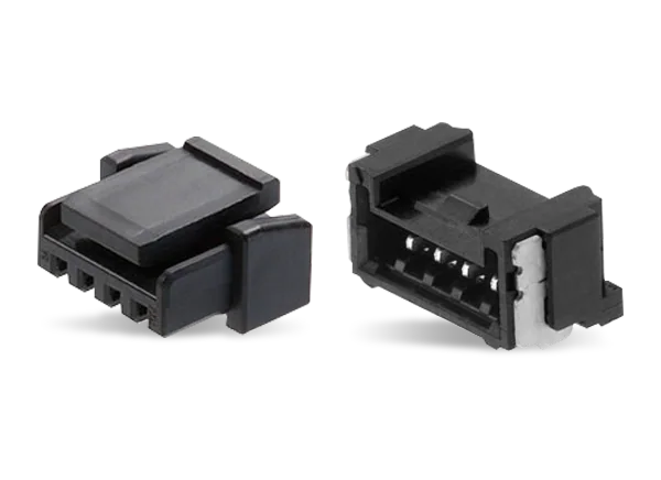
Sometimes, as part of hand PCB assembly, you may need to also hand-assemble a cable. For example, wire and crimp terminal cables can be used with plastic connector housing to create a custom cable assembly that connects two or more boards together.
Connectors like the Micro-Lock Plus from Molex can be hand assembled with wires and crimps as part of a custom cable assembly or wiring harness
If you are going to use hand-assembled cables and connectors, make sure there is a very clear wiring diagram that denotes pin numbers on the connector body. This is especially important if the connector is keyed and cannot be rotated or reversed. If the connector can be rotated, think about making your connector pinout rotation-proof. These steps will ensure that a hand assembler matches the right pins with the right wires.
Parts Kit With Designators
Last but not least, you can really help out your hand assembly technician if you have an appropriate parts kit. One thing you can do to speed up assembly is to write down the reference designators directly on the parts labels. This gives you an opportunity to give the BOM a fresh look and ensure all the correct parts were ordered, and it ensures there are no mistakes in placements during hand assembly.

Photo courtesy of Zach Peterson
Whether your team is creating advanced prototypes or transitioning a new product into manufacturing, Altium Designer® gives PCB designers everything they need to design for cost and quality. When you’re ready to share your outputs with your manufacturing house, you can use the Altium 365™ platform to collaborate across design and production.
We have only scratched the surface of what’s possible with Altium Designer on Altium 365. Start your free trial of Altium Designer + Altium 365 today.
About Author
Related Resources
Related Technical Documentation
Table of Contents
Design to Release, Without the Friction
- Keep reviews tied to the right version
- Reduce handoff confusion and rework
- Spot sourcing and release risk earlier
- Work solo, share when needed
Get Started
Thank you, you are now subscribed to updates.


