


Circuit Board Design for In-Circuit Testers


There are many types of circuit board tests available in electronics manufacturing today, each having unique goals and characteristics. This article presents guidelines at the design level (schematic and layout) to enable the use of in-circuit testing (ICT) fixtures to verify proper component assembly. These simple test fixtures allow your board to be tested as its assembled, which helps identify and remove failed boards from your production run.
The following checklists can be used when an in-circuit testing fixture will be developed for your design. These guidelines do not address flying probe testers, automated optical inspection (AOI) tools, X-ray or boundary scan technology.
Testability Checklist at the Schematic Level
Testpoints can be easily created in your schematic with the CAD tools in your schematic editor. Once you create your testpoints, there are several techniques that can be used in your schematic level to enable in-circuit testing and ensure reliability of the test:
- Tie IC control lines high or low using individual pull-up or pull-down resistors
- Tie unused inputs high or low using individual pull-up or pull-down resistors
- Include method to disable clocks (can be accomplished using jumpers, tri-state buffer or enable line of oscillator if available)
- Provide disable methods for programmable logic devices (PLDs), application specific integrated circuits (ASICs) and other custom devices
- Provide ‘disable methods’ for bussed devices, high current devices, Flash RAMs, EEPROMs, and D/A converters
- Provide circuitry to disable digital feedback loops
- Provide a means to disable on-board PROM
- Isolate power-on reset circuits from other digital circuits
Testability Checklist at the PCB Layout Level
Here are some design guidelines for testpoints that can be implemented in Altium Designer on the PCB side. Consider as many of the following ideas as possible to aid the tests being performed by your manufacturers:
- Keep components and test points at least 3.2 mm (.125) from board edges (preferably 3.8 mm or .150 in).
- Provide at least two unplated 3.2 mm (0.125) diameter tooling holes, preferably in opposite corners, and leave 3.2 mm annular area around them free of components and test points. Consider using a "keying" pattern so boards can't be inserted backwards.
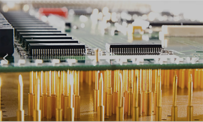
- A double-sided test fixture is more expensive, so try to put all test points on one side of the board, usually the bottom or the side with the least circuit complexity. If the top-side of the board must be used for probe sites, use top only for non-critical nets. Keep test points for clocks, control pins, programming pins, serial data and boundary scan on bottom.
- Test point sites can be through-hole leads, dedicated pads, or small diameter vias, but avoid placing test points on surface mount lands or gold-plated edge fingers. Don't use larger via diameters as test probe sites. Via hole size should be 0.36 mm (.014) or less.
- For 100% testability, provide at least one test pad for each net.
- Provide two pads on nets tied to critical low impedance devices (four-wire Kelvin testing).
- Provide 2-10 probe sites for primary power, and at least two test points for each isolated power/ground net. For primary ground provide many probe sites, consider one test point for every twenty grounds, or consider a grid of at least one per square inch.
- Probe sites with 1.0 mm (.040) pad diameters are preferred, 0.9 mm (.035) is acceptable, 0.8 mm (.031) can be used if tooling holes are available for alignment, but smaller diameters will reduce contact repeatability.
- Try to space probe sites at least 2.5 mm (.100) apart, center-to-center. In reality, 0.9 mm (.035) pads spaced 1.8 mm (.070) is considered standard by many. Closer spacing is possible but will require using thinner, less reliable and more expensive probes.
- Test points should be evenly distributed over the surface of the board. High stress in congested areas can cause boards to warp.
- Keep tall components on the side that is not probed. The platen has to be cut out in places where components are over 6.4 mm (.255) tall on the probed side. For these, keep test points at least 5.0 mm (.200) away.
- For components taller than 2.6 mm (.100), maintain minimum 2.0 mm (.080) clearance, edge-to-edge. For all other components, keep test pads at least 1.0 mm (.040) from component body, edge-to-edge.
- If component through-holes are used for test probe locations, make sure leads are robust enough for compressive force (be careful using LEDs or some types of transformers). Also, make sure PTH leads will be present on all versions of assembly (not depopulated).
- If design is panelized, try to include at least one tooling hole on each board in addition to the tooling holes in rails.
Configuring Testpoints for In-circuit Testing
Altium Designer® provides a Testpoint Manager to help analyze your design for testability.
Access this feature from the Main Menu>Tools>Testpoint Manager:

Revising Designs with Existing ICT Fixtures
Test fixtures are very expensive, but it is often possible to modify an existing fixture to accommodate a revision instead of developing new ones. If it is possible to use an existing fixture, it will be easier, faster and less expensive using the following guidelines:
- Do not move tooling pin holes.
- Do not move test points unless absolutely necessary.
- Do not put a new test point within 0.100" of an existing test point (or from a test point that is being removed).
- Do not rename existing components.
- Do not name new components with the same name as components that have been removed.
- If a connection on a net has changed, rename the net.
- If a net splits into two or more nets, don't re-use the old net name; create new net names.
- Even if the original testpoint diameter was smaller, try to increase the diameter of new test points up to 0.040" to ensure a reliable contact. (When fixture vendors re-drill holes for probe sockets into an existing fixture, they may not be as accurate as when the original fixture was fabricated.)
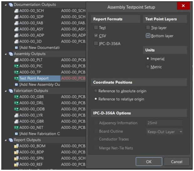
Creating a Testpoint Report for Manufacturing
The Altium Designer system can export the testpoint report, and this can be automated as part of your OutJob configuration:
Summary
Taking advantage of the ideas in this article will make your in-circuit testing programs easier to implement, will reduce the chance for error, and will make adjustments for revisions less expensive and more reliable.
DISCLAIMER: The advice given here should be understood as merely a guideline to get you started. The electronics industry moves quickly, and standards change constantly. If anything mentioned in the article above contradicts your own design process, consult with your manufacturing partners and make adjustments (if any) to suit your in-circuit testing process.
For More Information
Here is the Testability Standard published by the Surface Mount Technology Association:
SMTA-TP-101 TESTABILITY GUIDELINES
Altium Documentation
For more about how Testing is performed in manufacturing, see these two Altium blog articles by Kella Knack:
- PCB Design For Test—Test Structures And Types Of Tests, Part 1
- PCB Design For Test Structures And Tests Performed, Part 2
Would you like to find out more about how Altium can help you with your next PCB design? Talk to an expert at Altium.
About Author
Related Resources
Table of Contents
Design to Release, Without the Friction
- Keep reviews tied to the right version
- Reduce handoff confusion and rework
- Spot sourcing and release risk earlier
- Work solo, share when needed
Get Started
Thank you, you are now subscribed to updates.


