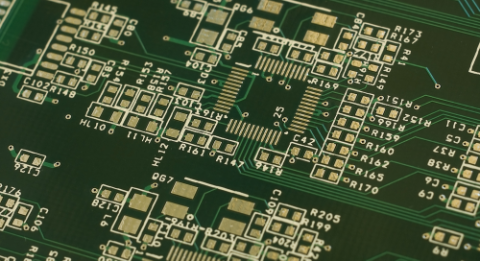
Getting Started With High Current PCB Design

Systems that operate with high currents or high voltages carry a unique set of challenges that are not seen in smaller digital systems. Operators could be exposed to unsafe conditions, and designs could fail due to heat or electrostatic discharge. However, the right PCB design decisions can help reduce the risks involved in interacting with power electronics. In this guide, we’ll look at some of the basic design points to be considered in high-current circuit board design. In some cases, the layout and safety considerations involved in high-current circuit board design are similar to those in high-voltage design, especially when we look at safety. Here are some high-current PCB design tips.
The Basics of High Current Circuit Board Layouts
There are some good examples of high-current PCB designs that aren’t necessarily operating at high voltage. Also, the very idea of “high voltage” vs. “high current” is somewhat arbitrary. Probably the best metric to distinguish these types of designs are in terms of safety. If there is a risk of electric shock or overheating due to DC current, then you may need to apply some of these design principles to ensure safety and reliability.
Component Selection
High-current board designs and high-power PCB systems in general get much of their reliability from components. As obvious as it might sound, make sure you factor in a safety margin for components during selection. In general, it’s best to start by looking at two specifications:
- Current ratings, particularly for MOSFETs and inductive components
- Thermal resistance values if available
You can use the estimated or designed operating current to determine power dissipation, or the first specification above to get a worst-case value. Both of these will help with thermal management, which requires using the thermal resistance value to estimate temperature. For some components, you can then determine whether a heat sink is needed to ensure reliability.
Other components that are important for high-current circuit boards, such as connectors, can have very high ratings and will be useful in high-power PCB systems. Two examples of mechanical screw terminal connectors that can handle very high currents are shown below.

Choose the Right Copper Weight
The resistance of copper used in traces creates some DC power loss, which is dissipated as heat. For very high current PCB layout connector design, this becomes very important, particularly when component density is high. The only way to prevent DC losses in a high-current PCB is to use copper with a larger cross-sectional area. This means, either heavier copper is needed, or traces need to be wider to keep Joule heating and power loss low enough. Use a PCB trace width vs. current table to determine the copper weight and/or trace width required to prevent excessive temperature rise.
Going Bigger: Use Planes Instead of Traces
If you have to get very high currents into a power system, and traces are just getting too wide to accommodate your needs, use power planes instead of traces. Just as an example, in Eurocard format backplanes we’ve done in the past, we used multiple power planes to supply 100 A of current from two dedicated low-voltage (24 V max) power supplies. You can use the same strategy in other systems when you need to support extreme currents.
Thermal Vias With Copper Pour
Inside a circuit board enclosure with stagnant air, heat transfer away from the device can be difficult if you only rely on conduction or natural convection. Thermal vias can be placed in the board with copper on the surface layer to provide additional heat transfer away from some components by providing a direct connection to a plane layer (GND). This can be used on circuits near hot components or traces just to provide some additional heat conduction away from the surface layer, but it should not be used in cases where isolation is required, such as between the primary and secondary turns in a power transformer.
Although thermal vias are good for targeting specific components, the better strategy is to consider how to use a large heat sink or a direct conduction path to the enclosure to provide high heat dissipation. An example is shown below for a bank of MOSFETs in parallel.

Pay Attention to Ground
High-current systems may need to use the same kind of safety fault measures. Some level of safety and EMI can be achieved with a proper grounding strategy. Normally, you should not split up grounds, but power systems involving high current and/or high voltage are an exception. Grounds need to be split between the input AC, unregulated DC and regulated DC sections.
A good place to start is with the grounding strategies you’ll find in AC systems or isolated power supplies. In general, for high-current power systems, you will have a 3-wire DC arrangement (PWR, COM, GND), where the GND connection is really an earth connection. Your board might use an isolated strategy, where the output side is disconnected from GND, while the input side is earthed to ensure safety in the event of a fault. Read more about implementing a grounding strategy for safety in this article.
Use a Thicker Circuit Board
At first, this might seem counterintuitive. You would think that a thinner board provides greater conduction away from components, so why use a thicker board? In fact, the in-plane thermal resistance will be lower and the thermal mass of the board will be higher when a non-standard board thickness is used. Thicker boards (2 or 3 mm) can also provide greater mechanical support for bulkier components in a high-current circuit board, particularly board-mounted inductive components and large heat sinks.
ESD and Safety
This portion of a DC presents its own set of problems, particularly in power systems, and especially in designs operating at high voltage and high current PCB layout connectors simultaneously. To learn more about ESD protection in power systems operating at high voltage, read this guide on the common ESD circuit designs. In an upcoming article, we’ll look at some of the basic points involved in high-voltage circuit boards from the viewpoint of materials selection and layout. These boards carry some of the more important safety challenges, especially when they are capable of sourcing high currents.
Whether you need to design a high voltage or high current PCB circuit board, use the PCB design tools in CircuitMaker to prepare your schematics and your PCB layout. All CircuitMaker users can create schematics, PCB layouts, and manufacturing documentation needed to move a design from idea to production.
Start using CircuitMaker today and stay tuned for the new CircuitMaker Pro from Altium.


