PCB Thermal Resistance: Theory and Management

The thermal conductivity of your PCB material stackup and arrangement of copper conductors are important factors that determine the thermal performance of your circuit board. You will likely need to include strategically placed thermal vias, a heat sink on each active component and power electronics, and active cooling measures near any other heat source on your circuit board. Copper in printed circuits has high thermal conductivity, while FR4 and other substrate materials have much lower conductivity, and proper layout and component selection can aid heat transfer as part of thermal management.
When you receive a test coupon, for your board, you may need to measure the thermal conductivity of your PCB material as part of the design process. This can help inform any redesigns and determine whether you need to include more thermal vias, planes on interior layers, or other cooling methods to remove heat from your board. It can also help determine whether you should rearrange components on your circuit board.
With the right circuit board substrate material and component choices, you can devise a thermal management strategy that can help control heat transport in your board. Using proper arrangement of copper elements, components, and interior plane layers, your thermal management strategy can remove transport heat away from each heat source and bring your printed circuit board temperature closer to ambient temperature. You should inform these design choices through measurements of thermal resistance of your PCB and try to reduce the thermal resistance as much as possible.
ALTIUM DESIGNER
A unified PCB design package that integrates advanced PCB design and layout features with a comprehensive substrate material library and production planning features.
The material properties of your circuit board substrate and conductors determine the thermal performance of your circuit board and should inform your thermal management strategy during PCB design. One of the most important material properties, especially in power electronics devices and high-speed devices, is the effective thermal conductivity of your circuit board. This is determined, in part, by the thermal conductivity of your substrate material, conductors in a printed circuit, the junction temperature of active components, and the location of each heat source in your system.
When excessive heat accumulates in particular locations in your circuit board, your components and portions of the substrate will rise to high temperatures. This can cause fracture of high aspect ratio vias and failure of active components. As part of your thermal management strategy, you’ll need to determine the best component arrangement, thermal via arrangement near components, and determine which components will benefit from a heat sink or cooling fan.
What is PCB Thermal Resistance?
Thermal conductivity is sometimes incorrectly interchanged with thermal resistance. Just like resistivity and conductivity of electrical components have an inverse relationship, the same goes for PCB thermal conductivity and thermal resistance. The thermal resistance of your PCB is determined by the material properties of your substrate and the arrangement of copper elements in your board. Overall, this defines the rate of heat transfer between hot a cold regions of your PCB.
As copper is a conductor, it also has high thermal conductivity (this is the case with most electrically conductive materials), and the copper elements in a printed circuit will provide a low thermal resistance path for heat to move away from a heat source. As the thermal conductivity of FR4 and other common substrates is quite low, copper in a printed circuit will transport heat through the board much faster than heat will naturally conduct through the substrate. This combination of a high thermal resistance material (FR4) and a low thermal resistance material (copper) determines the effective thermal conductivity of a printed circuit board.
Methods of Measuring Thermal Resistance of PCBs
Thermal resistance is normally determined by measuring the thermal conductivity of a finished PCB. The thermal conductance is easily calculated from the thermal conductivity, and the thermal resistance is the inverse of the thermal conductance. As PCB substrates are two dimensional, the thermal conductivity of a finished, unassembled circuit board is best measured using the guarded hot plate method, or the 3-omega method can be used with smaller circuit boards.
The guarded hot plate method is by far the easiest method as you simply measure the temperature on two sides of a board as heat transfers from the hot side of the circuit board to the cold side. This provides a simple way to directly measure the thermal conductance, which can then be used to calculate thermal conductivity and thermal resistance.
The 3-omega method is a thermoelectric method, where the board is heated with an AC heater at a specific frequency. This induces periodic heating at double the frequency. The measured temperature signal will contain components at the heating frequency and triple the frequency, this is the name “3-omega.” The thermal conductivity of the test coupon is proportional to the strength of these frequency components and the geometry of the test coupon. Some excellent information on this method can be found in this publication.
- Your thermal resistance measurements should inform a larger thermal management strategy for your circuit board. Learn more about devising a thermal management strategy.
- Your layer stack determines the effective thermal conductivity of your circuit board. The right layer stack can aid heat transfer away from active components and help prevent signal integrity problems.
- Ceramic and metallic substrates have higher thermal conductivity than FR4 and other laminates. You might consider using an alternative printed circuit substrate material with higher thermal conductivity. Learn more about selecting the right substrate material for thermal management.

3D view showing power dissipation and heat accumulation in a printed circuit
Your Thermal Management Strategy
Defining a stackup is just one important aspect of designing your board to have higher effective thermal conductivity. The materials used in your stackup will help determine the overall thermal resistance and resulting heat transfer rate in your board. The arrangement of copper conductors and the use of heavier copper can help transport heat from components that generate a large amount of heat.
Depending on the environment where your board will be deployed, different design choices may be necessary to ensure the temperature of your board and components stays closer to ambient. With active cooling measures, you may need to make sure the required components do not generate excessive noise in nearby circuits. Most likely, you will need a combination of passive and active heat dissipation tactics to bring the temperature of your board closer to the ambient temperature and ensure the temperature distribution in your circuit board is more uniform.
Developing a Thermal Management Strategy
Judicious placement of thermal vias, active cooling devices like fans, and an appropriate arrangement of components will all aid heat transport around your circuit board. In a circuit board that contains a large number of active components, you can help prevent hot spots by placing these components away from the edge of the board, and by not clustering them in one location. When used with thermal vias and planes in interior layers, your temperature distribution should become more even during operation.
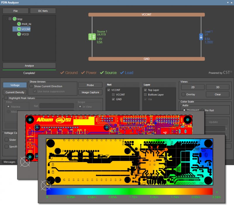
A thermal simulation tool can also help you determine the best thermal management strategy for your PCB. One aspect is tracking power dissipation throughout your PCB to get an idea of how your PDN acts as a heat source. When used alongside the power ratings for your component values and your thermal resistance measurements, you can get an idea of how heat will move through your board and the final temperature distribution.
- Placing a heat sink on an active component that generates significant heat is an important part of a passive cooling strategy. This helps you compensate for a circuit board with high thermal resistance by moving heat into the surrounding air rather than into the board. Learn more about thermal pads and thermal paste for attaching a heat sink.
- Your layer stack should be designed with an eye for thermal management in your circuit board.
Learn more about working with a layer stack manager in your PCB design software.
- Working with a PDN analyzer tool can help you identify potential hot spots and track power dissipation in your power density network.
Learn more about working with a simulation-driven workflow in PCB design.

PDNA simulation showing power dissipation in Altium Designer
Best Software for Managing Thermal Resistance of PCBs
The best software for managing thermal resistance of your circuit board will contain a complete set of layout tools, as well as access to a huge component library that allows you to easily place a heat sink on important components and active cooling components in your board. The best software for designing for low thermal resistance will include integrated these tools in a single program. You shouldn’t have to use separate PCB design programs for stackup design, PCB layout design, and simulation.
Integrated Design in Altium Designer
Altium Designer includes a complete set of layout and routing features that are integrated with your layer stackup manager, allowing you to customize your layout for use with alternative substrate materials. This simplifies your PCB design process as you can create a board with a high thermal conductivity substrate and immediately import it into your PCB design editor.
Altium Designer includes plenty of other tools for PCB design beyond stackup and routing. You’ll have access to a complete set of production planning tools that allow you to quickly generate deliverables for your manufacturer. The data management tools also help ensure your component data does not go stale and provides revision tracking features without incorporating a 3rd party application. The simulation tools will immediately take your PCB design data and perform a large number of analyses.
- Altium Designer’s integrated design features offer a complete set of layout, routing, simulation, and documentation features in a rules-driven design engine. Altium Designer makes it easy to define your stackup, component arrangement, and PCB layout in a single application. Learn more about Altium Designer’s integrated design environment.
- Altium Designer’s stackup material library allows you to select from a large number of standard materials for use as your PCB substrate. You’ll be able to easily define your layer stack and via designs in Altium Designer. Learn more about the materials stackup library in Altium Designer.
- The routing features in Altium Designer are designed to automate or semiautomate your layout, helping you stay productive as you implement your thermal management strategy. Learn more about the interactive routing tools in Altium Designer.
Altium Designer’s CAD tools are unique in that you can easily arrange components and devise a routing strategy to minimize the thermal resistance of your circuit board. When used with the materials library and stackup manager, you’ll have a complete set of design tools for thermal management in your circuit board.
Altium provides every designer with the resources they need to get started using the powerful design features and create new technology successfully. You’ll have access to the AltiumLive forum, webinars and podcasts with industry experts, an extensive knowledge base, and design tutorials with plenty of design tips. No other PCB design software company is this invested in your success.
Altium Designer has set a new standard in integrated circuit board design and analysis. Rather than working in separate applications, you’ll have access to a complete set of routing, layout, management, and production tools in a single interface. You can easily pass PCB design data between these important features and take control over all aspects of your product. It’s time to take your design productivity into overdrive with Altium Designer.


