








Let GreenPAK Replace Your Buck and Boost Converters

At a Glance
Buck and boost converters are easy to design and implement from discrete circuits, but boost converter controllers offer limited functionality. GreenPAK brings a host of new functions to boost converter designs that aid higher-bandwidth power delivery and low-noise operation.


Buck and boost converters are fundamental DC/DC power conversion circuits. Buck converters step higher voltages down to lower logic levels, while boost converters step lower voltages up to higher values, with both often used alongside batteries to maintain stable system rails. This is all based on PWM driving while sensing the output with a feedback loop. Compact buck and boost converter controllers make this a very simple implementation, sometimes with integrated FETs for switching or with external FETs for higher power delivery.
Although there are many compact buck and boost converter controller options, and even some highly integrated components with internal switchers, the feature depth they offer for noise control and power monitoring is almost nonexistent. Many offer a soft-start option, compensation tuning, and thermal shutdown/short circuit protection, but that is about it.
When systems get more compact and feature demands increase, an alternative controller type is needed, and that’s exactly what you’ll find in mixed-signal processors. These parts can easily implement buck and boost converter controllers, and we’ll show how this works in this article.
Basic Buck and Boost Converter Topologies
Buck Converter
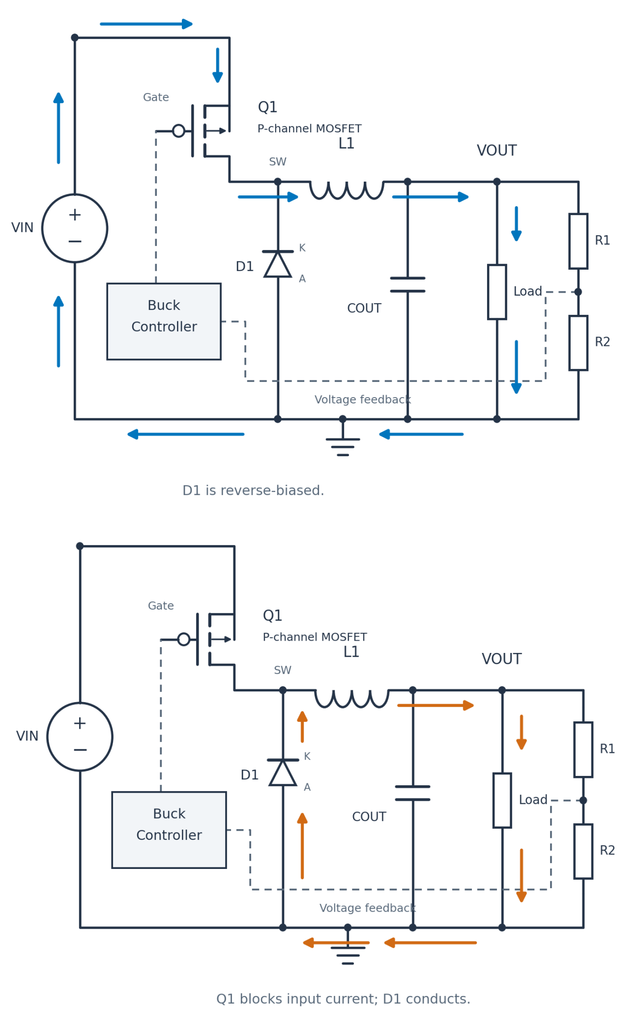
A basic buck converter places a switching MOSFET between the input supply and an output inductor. When the MOSFET conducts, the voltage across the inductor causes its current to rise while supplying the load. When the MOSFET turns off, current continues through a freewheeling diode or synchronous low-side MOSFET. The output capacitor filters the inductor current ripple and helps to supply the current demanded during load transients.
The controller senses the output through a resistor divider and adjusts PWM duty cycle to maintain the feedback reference voltage. For ideal continuous-conduction operation, the output voltage equals the input voltage multiplied by duty cycle. Switching frequency and inductance determine current ripple, while capacitance and control loop response determine how quickly the converter can respond to load changes.
Boost Converter
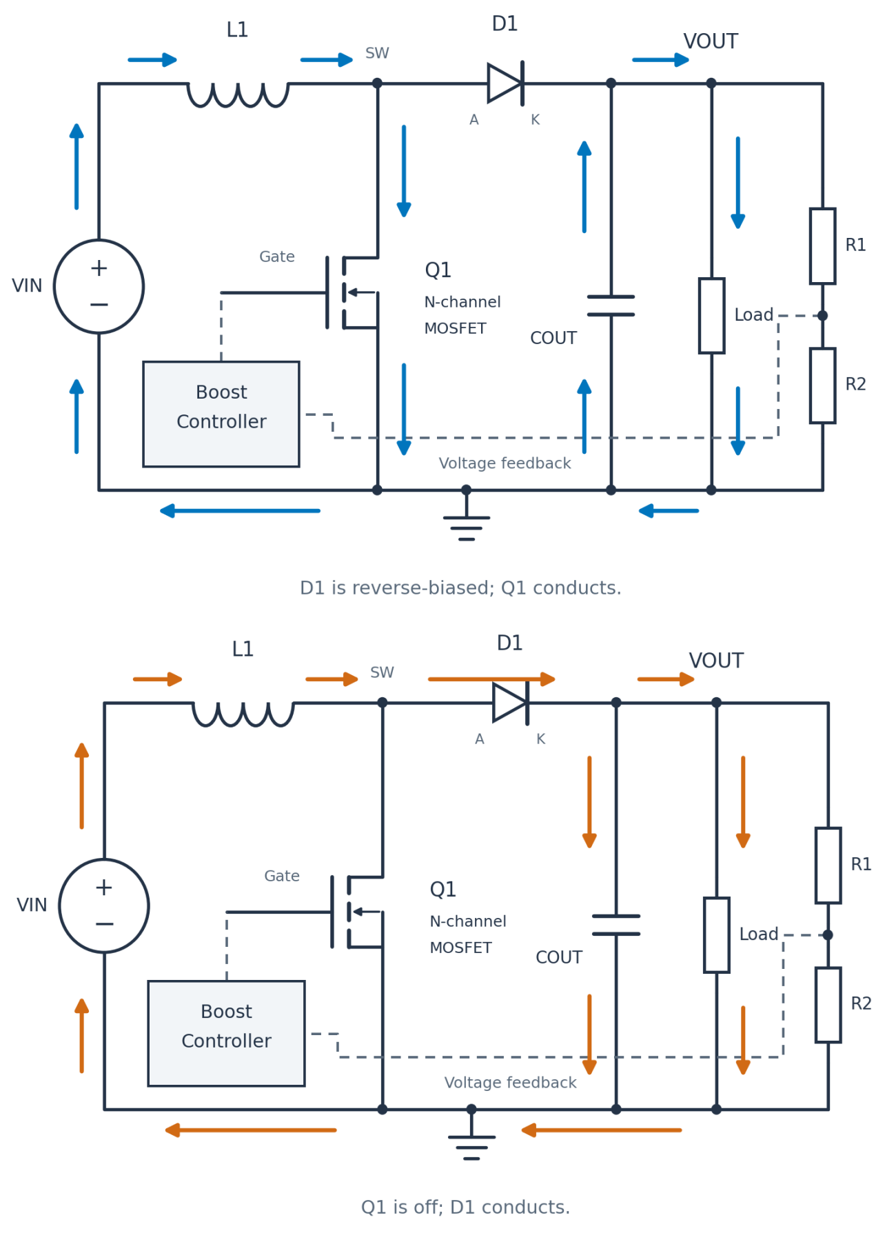
A basic boost converter connects an inductor between the input supply and a switching node. A low-side MOSFET pulls that node toward ground during the on interval, increasing inductor current while the output capacitor supplies the load. When the MOSFET turns off, inductor current flows through a diode into the output capacitor and load. The switching-node voltage rises above the input voltage to sustain this current path.
The controller measures the divided output voltage and adjusts switching duty cycle to maintain regulation. Ideally, continuous-conduction operation gives an output voltage equal to the input voltage divided by one minus duty cycle. Increasing the conversion ratio raises input current for a given output power, increasing conduction losses and inductor current requirements. The MOSFET and rectifier therefore require voltage ratings above the regulated output, with margin for switching overshoot under expected operating conditions.
Standard Controller Features
Common controller functions manage startup, switching, and fault conditions. Their implementation determines how the converter behaves during supply ramping and overloads:
- Soft-start controls the output voltage ramp and associated capacitor charging current
- Undervoltage lockout prevents operation below the required supply voltage
- Current limiting restricts switching or inductor currents
- Thermal shutdown protects the controller against excessive die temperature
- Enable inputs support external startup and shutdown control
Advanced Features in Buck and Boost Converter Controllers
Advanced buck and boost controllers provide additional control over switching noise, efficiency, and coordination between power rails. Some of these features are outlined below.
Spread spectrum | Controlled switching frequency modulation | Reduces spectral peaks; requires ripple evaluation |
Clock synchronization | Switching locked to an external clock | Coordinates converters and sensitive frequency bands |
Multiphase operation | Phase-shifted parallel power stages | Distributes heat and reduces ripple (depending on duty cycle) |
Zero-voltage switching | Resonant transitions that are timed to gate modulation | Reduces turn-on loss within defined operating conditions |
Buck and Boost Converter Control With GreenPAK
Advanced buck converter controllers integrate even more features than the advanced features list above, but these are often implemented with a host microcontroller and a set of peripheral components. These and many other features can be aggregated into a single controller ASIC with GreenPAK by Renesas, a programmable mixed-signal processor platform.
The SLG47105 combines analog comparators, oscillators, configurable logic, and high-current bridge outputs, all of which are configurable as a custom buck converter controller. The image below shows a multi-rail buck converter example from the GreenPAK Cookbook in the Go Configure development suite. An analog comparator, lookup table, D flip-flop, and counter/delay block are used to generate the switching control signal for a buck converter, while other pins pass power to the switch node and sense the output voltage to ensure the target voltage is maintained.
The boost example shown below uses an external low-side MOSFET, inductor, and Schottky diode to step up the output rail. The external MOSFET gate is driven through an external resistor, while a ACMP0H compares the output voltage feedback line against a 1.920 V reference.
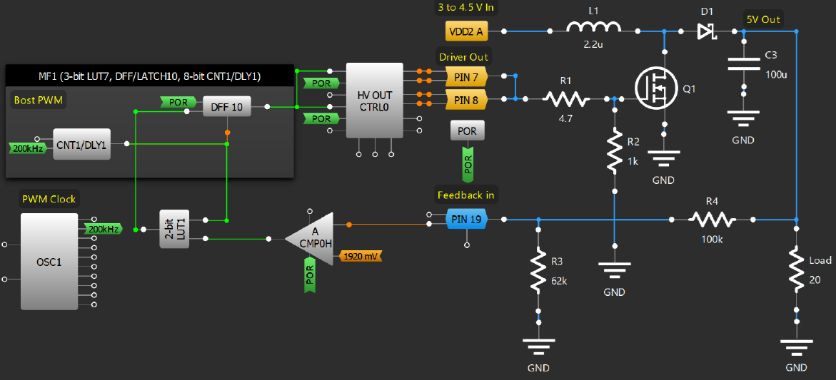
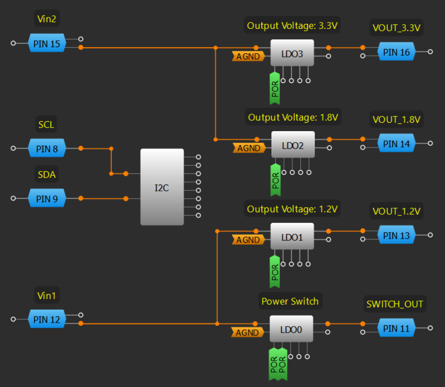
GreenPAK devices do much more than provide buck converter control. A designer can aggregate multiple capabilities into one IC, including power monitoring, regulator sequencing, and sensor interfaces, and settings can be reconfigured through a serial interface.
The Go Configure development suite allows engineers to configure comparator thresholds, qualification logic, delays, and output behavior. Simulation and development hardware support evaluation of the resulting sequence, including early requests and interrupted settling. Device selection depends on the analog resources, timing blocks, and pins required for each independently controlled enable output.
To learn more, take a look at the GreenPAK components and reference examples.
Whether you need to build reliable power electronics or advanced digital systems, use the complete set of PCB design features and world-class CAD tools offered by Altium to implement your GreenPAK solutions. Altium provides the world’s premier electronic product development platform, complete with the industry’s best PCB design tools and cross-disciplinary collaboration features for advanced design teams. Contact an expert at Altium today!
Related Resources
Related Technical Documentation
Thank you, you are now subscribed to updates.