










The World's Smallest Analog Interface - Built With GreenPAK

At a Glance
See how GreenPAK reduces analog interface PCB area and how the upcoming SLG46801 combines WLCSP packaging with in-system reprogrammability.


Small analog interfaces often consume more PCB area than their schematics suggest. A sensor threshold detector may require comparators, timing circuitry, a latch, and logic to generate an interrupt or control signal. Each component adds its own footprint, placement clearance, and routing. In a wearable or compact sensor module, these supporting circuits compete with the battery, antenna, and mechanical features for space.
GreenPAK reduces this area by combining analog detection, timing, and configurable logic inside one small package. This allows engineers to consolidate an entire interface function, including the circuitry that qualifies an analog event before the host responds. Existing GreenPAK devices already support this approach in packages occupying only a few square millimeters, while the upcoming SLG46801 adds a smaller WLCSP option and in-system reprogrammability.
Analog Interface Integration
Consider a sensor interface that asserts an interrupt when its output exceeds a threshold for a specified duration. A discrete implementation could use a comparator, timer, and logic that combines the qualified event with an enable signal. A latch might retain the event until the host acknowledges it. GreenPAK devices with suitable resources can implement these functions through their internal comparators, counters, LUTs, and flip-flops.
This kind of consolidation extends beyond a latching sensor interface. Examples include detecting a supply threshold, qualifying a sensor alarm, or enabling another circuit after a delay.
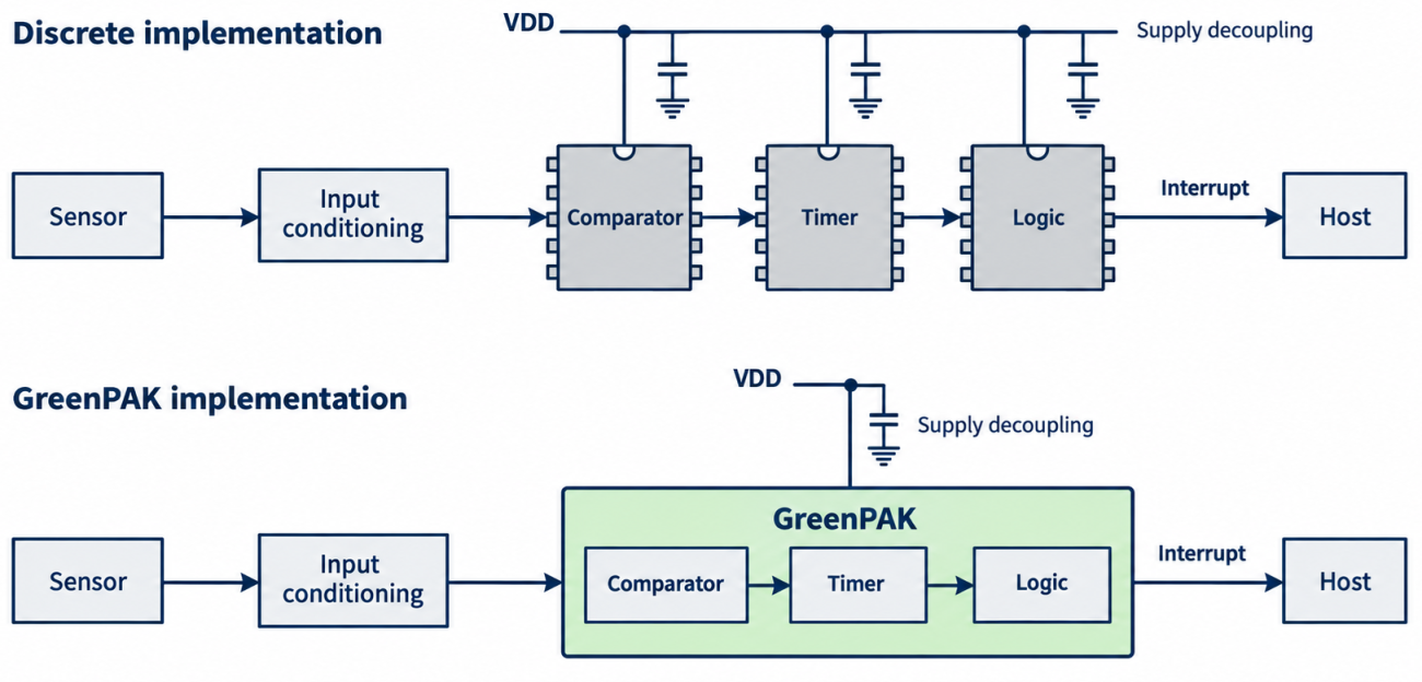
The integration also removes intercomponent connections from the PCB. Comparator outputs and timing signals can travel through the internal connection matrix, reducing the number of traces routed around the sensor interface. This gives the designer more freedom to keep analog inputs, including low-SNR signals, separated from noise sources on the PCB.
Existing GreenPAK Package Sizes
Several existing GreenPAK devices demonstrate how much functionality fits into a small package. Three examples are given below, with minimum leadless package (STQFN) size of 1.6 mm × 1.6 mm. Devices with additional analog or power functions remain compact, allowing package selection to follow the circuit requirements.
Example device | Small package option | Package body area | Relevant integrated resources |
SLG46120 | 1.6 mm × 1.6 mm STQFN | 2.56 mm² | Two comparators, logic, counters, and delays |
SLG46116 | 1.6 mm × 2.5 mm STQFN | 4.00 mm² | Two comparators, logic, timing, and a P-channel power switch |
SLG46620 | 2.0 mm × 3.0 mm TQFN | 6.00 mm² | Six comparators, an 8-bit SAR ADC, two DACs, and logic |
As an example comparison, assume that an analog front-end requires separate comparator, timer, and logic ICs each occupying a 2 mm × 2 mm package size; their combined body area is 12 mm². Consolidating equivalent functions into a 1.6 mm × 1.6 mm GreenPAK device would reduce that area to 2.56 mm², or ~79% reduction in board area.
Before committing to the smallest package, verify:
- Match comparator input range to the supply voltage selection, and determine hysteresis/response time against the sensor requirements.
- Available pins and macrocell assignments for the complete interface.
- Timing tolerance, startup behavior, output loading, and assembly requirements.
SLG46801 in WLCSP
The upcoming SLG46801 extends this integration approach with multi-time programmable memory and two announced package options: a 1.6 mm × 1.6 mm STQFN and a 1.155 mm × 1.155 mm WLCSP. The upcoming WLCSP devices will occupy approximately 1.33 mm², about 48% less area than the STQFN option.
The SLG46801 integrates two high-speed analog comparators, configurable logic, counters, delays, and oscillators. Its preview datasheet specifies a 1.71 V to 5.5 V supply range for both operation and programming. I²C provides access for in-system reprogramming, allowing supported logic and timing configurations to change after deployment. The announced dynamic sharing of GPIO and I²C functions also helps designs with limited pin availability.
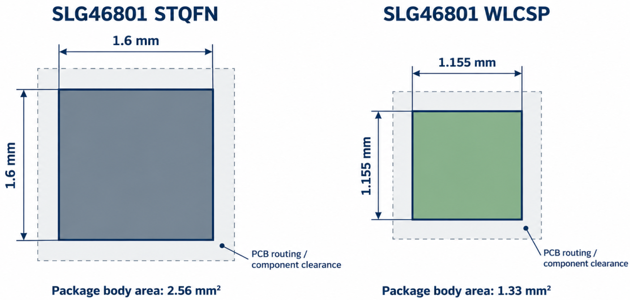
The new SLG46801 devices also allow for multi-programmability, meaning a device could be reconfigured on-the-fly during operating. For a sensor interface, reprogrammability can support revised event qualification or control behavior without replacing components.
WLCSP selection should include a review of the recommended land pattern, solder-mask geometry, routing rules, and assembly capability. Engineers can evaluate the interface architecture now and use the production package documentation to finalize layout. The largest area savings come from consolidating the interface first, then selecting the smallest package that the board and assembly process can support.
Use GreenPAK for Compact Analog Control Interfaces
Reset and wake-sleep controllers are practical examples of the analog interface consolidation described above, but of course there are many other analog sensing applications offering consolidation opportunities. Supply monitoring, threshold detection, event qualification, and reset timing can share one GreenPAK device, reducing the separate ICs and interconnections needed around a host processor.
On-chip comparators detect analog conditions, while configurable LUTs, flip-flops, and counters determine when to assert a reset, enable a circuit, or wake the host. These hardware functions can operate without a separate firmware control loop, allowing the processor to remain asleep until a qualified event requires its attention.
The Go Configure development tools allow engineers to configure these functions around their application requirements. Device selection should account for the required analog resources, timing behavior, and available pins before choosing the package. The SLG46801 adds in-system reprogrammability for supported configuration changes while extending this integration approach to WLCSP.
To learn more, take a look at the GreenPAK components and reference examples.
Whether you need to build reliable power electronics or advanced digital systems, use the complete set of PCB design features and world-class CAD tools offered by Altium to implement your GreenPAK solutions. Altium provides the world’s premier electronic product development platform, complete with the industry’s best PCB design tools and cross-disciplinary collaboration features for advanced design teams. Contact an expert at Altium today!
Related Resources
Related Technical Documentation
Thank you, you are now subscribed to updates.

