








HV Load Driving and Control PCBs With GreenPAK

At a Glance
Complex electronics often demand a complex system reset procedure in the event of faults or when users require a my preset. Here's how you can implement system resets without a microcontroller.


One of the biggest challenges in high voltage PCBs is switching and driving high voltage to a load. High voltage designs come with safety concerns as well as EMC challenges related to switching behavior. Switch-mode power supplies, motor controls, and high voltage control boards all require controlled switching, and they often require direct measurements of current and voltage at the load.
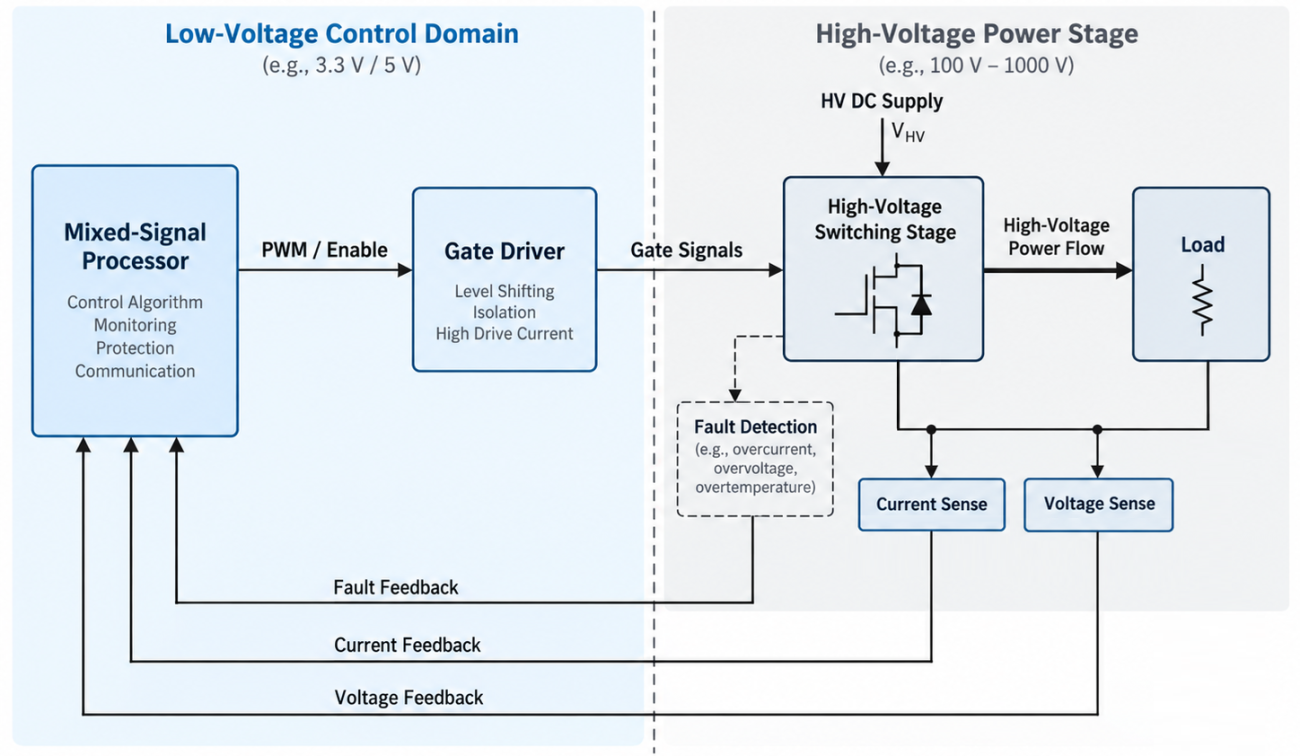
These functions are commonly divided among gate drivers, current sense amplifiers, and a microcontroller. A programmable mixed-signal processor can consolidate PWM generation, timing, sensing logic, and fault handling into one control device. This keeps the high voltage switching stage separated from the low voltage control domain while reducing the amount of supporting control logic.
High Voltage Load Controller Architecture
A practical controller places the mixed-signal processor between the system controller and the gate driver. The processor generates switching commands, monitors feedback, and determines when the power stage should be enabled or disabled. The gate driver still provides the gate voltage, source and sink current, isolation, or level shifting required by the switching devices.
Function | Typical Implementation | Main Design Constraint |
PWM generation | Mixed-signal processor | Frequency and duty cycle |
Gate drive | Dedicated gate driver | Gate voltage and peak current |
Threshold detection | Sense circuit and comparator | Accuracy and response time |
Fault shutdown | Hardware logic and latch | Deterministic response |
Restart control | Timer and state logic | Prevent repeated stress |
Gate Driving for High Voltage Loads
Modern high voltage power stages are commonly built with silicon MOSFETs, although newer designs are increasingly using SiC or GaN FETs, especially at high voltage. The mixed-signal processor controls when these devices switch, but it normally does not drive their gates directly. A dedicated gate driver is required between the control logic and the power FETs.
The driver has to be selected around the switching device and topology. Gate voltage, peak drive current, isolation requirements, and common-mode transient immunity can all affect switching behavior. The control logic establishes the timing, while the driver and gate network determine how quickly the device actually turns on and off.
PWM Generation and Switching Control
PWM generation is well suited to programmable hardware because switching frequency, duty cycle, enable timing, and pulse sequencing can all be implemented with deterministic logic. Counters, oscillators, comparators, and configurable logic can generate the switching waveform without relying on a continuously executing firmware loop.
The same logic can enforce startup conditions before PWM is enabled. Switching can remain disabled until the gate-driver supply is valid, the bus voltage is within range, and no fault inputs are active. Timers or controlled enable sequences can also prevent the power stage from transitioning immediately into its final operating condition.
These behaviors should be designed around the power stage. Irregular startup, asynchronous enable signals, or poorly controlled restart sequences can produce large current transients and unpredictable switching events.
Timing, Sensing, and Fault Protection
Half-bridge and full-bridge stages require non-overlapping gate signals. Programmable delays can establish dead time so that one device is fully off before the opposite device turns on. The required value has to include gate-driver delay, switching time, gate resistance, and component variation.
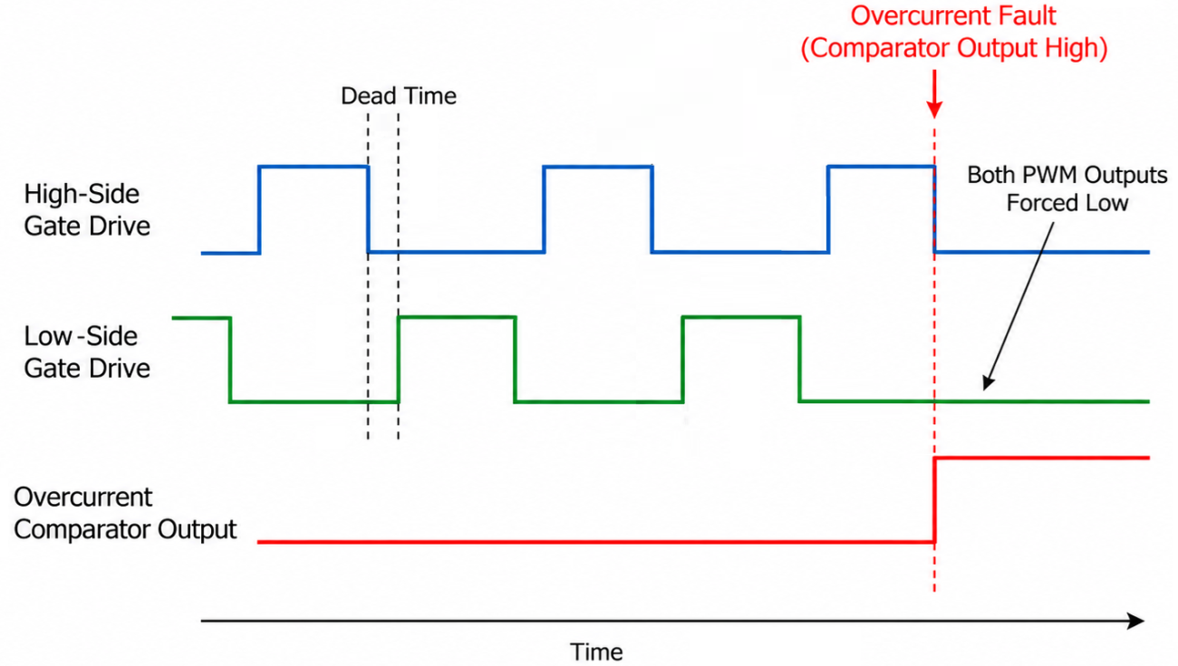
The same processor can monitor load current, bus voltage, temperature, and gate-driver fault outputs. Many protection functions only require a threshold decision, which makes an analog comparator preferable to a full ADC measurement when response time is the main constraint.
Typical hardware fault inputs include:
- Overcurrent or short-circuit detection
- DC bus overvoltage or undervoltage
- Overtemperature detection
- Gate-driver fault outputs
These signals can feed directly into the PWM disable path or a fault latch. This avoids the latency associated with ADC acquisition, an interrupt, and a firmware routine. After shutdown, the control logic can maintain a latched-off state or perform a timed retry depending on the allowable stress in the FETs, load, and power source.
EMI-Aware Switching Control
High voltage switching stages can produce conducted and radiated EMI through large dv/dt and di/dt events. Silicon MOSFETs can generate drain ringing and reverse-recovery current during hard commutation. SiC MOSFETs increase dv/dt, which can drive common-mode current through parasitic capacitances. GaN stages switch even faster, making small gate-loop and commutation-loop inductances capable of producing overshoot and high-frequency ringing.
The switching edge is therefore the main control variable. Faster transitions reduce switching loss, but they also increase transient current, voltage overshoot, and emissions bandwidth. Edge rate should be treated as a tunable design parameter rather than fixed at the fastest setting available from the gate driver.
A programmable mixed-signal processor can control several practical edge-rate adjustment methods:
- Select between multiple gate resistors with analog switches or small FETs.
- Control gate-driver strength or slew-rate mode pins.
- Select separate turn-on and turn-off resistance paths.
- Apply staged gate-drive commands when the driver supports multiple current levels.
These controls allow switching behavior to change with operating conditions. Final settings should be verified at the gate and switching node because PCB parasitics, driver behavior, and device characteristics determine the actual dV/dt and dI/dt.
Use GreenPAK for High Voltage Load Control
Renesas GreenPAK simplifies high voltage load control by integrating PWM generation, analog monitoring, timing, and protection logic into a single programmable device. On-chip comparators, voltage references, counters, and configurable logic can handle current thresholds, bus voltage monitoring, startup conditions, and fault detection without requiring separate control ICs for each function.
Configurable LUTs, flip-flops, delay elements, and counters can generate switching sequences, dead time, shutdown behavior, and controlled restart logic directly in silicon. Without additional firmware to maintain or boot time delays, GreenPAK provides a deterministic control solution that can reduce board space and simplify the low-voltage control circuitry around the gate driver.
The Go Configure developer tools give designers the ability to develop fully custom switching and protection logic that can also control gate-driver enable, slew-rate selection, or programmable gate-drive settings. These programmable mixed-signal processors allow high voltage power stages to combine sensing, timing, protection, and switching control in a smaller control architecture.
To learn more, take a look at the GreenPAK components and reference examples.
Whether you need to build reliable power electronics or advanced digital systems, use the complete set of PCB design features and world-class CAD tools offered by Altium to implement your GreenPAK solutions. Altium provides the world’s premier electronic product development platform, complete with the industry’s best PCB design tools and cross-disciplinary collaboration features for advanced design teams. Contact an expert at Altium today!
Related Resources
Related Technical Documentation
Thank you, you are now subscribed to updates.

