Embedded Capacitance Materials Overview

Capacitance is your friend whenever you need stable power integrity, which is why there is so much focus on decoupling capacitors. While these components are important and they can be used to provide targeted power integrity solutions to certain components, there is one specialty material used to supercharge capacitance in your PCB stackup or package substrate. This type of specialty material is called an embedded capacitance material, or an ECM.
These laminates can be incorporated into a PCB stackup to provide very high capacitance that aids power integrity. These materials can also act as a replacement for a group of decoupling capacitors if needed. This article will examine proper usage of these materials, as well as their material properties when used in IC substrate packages and PCBs.
What is an Embedded Capacitance Material?
Embedded capacitance materials are copper-clad laminates with very thin layer thickness and high dielectric constant. These materials are meant to separate a power and ground layer in a PCB stackup, thereby providing some capacitance that is embedded into the PCB stackup. Embedded capacitance materials are defined and described in the IPC 4821 standard (Specification for Embedded Passive Device Capacitor Materials for Rigid and Multilayer Printed Boards).
These materials provide two basic functions:
- Provide high plane capacitance in a PDN through their high Dk value and low thickness
- Provide damping for electromagnetic waves through their moderately high loss tangent
The main function of these materials is to provide higher capacitance in a PDN (giving lower PDN impedance) and greater damping for power bus ripple (leading to less intense power plane/cavity resonances at GHz frequencies) due to the material’s higher loss tangent. From a circuit perspective, these materials provide damping and capacitance simultaneously but with low spreading inductance, so they act like a controlled-ESR capacitor.
Improved Power Integrity
An example showing the effects of an ECM on power integrity is shown in the PDN impedance data below. In this graph, we can see quite clearly that the presence of a thinner ECM material lowers the PDN impedance as expected. The thinner material with a high loss tangent also damps the PDN resonances, as illustrated in the smaller peaks near 1 GHz, which is exactly in the frequency range where IC packages require fast pulse responses in the PDN.

The above result occurs because a thinner ECM provides more capacitance, but it does not provide more inductance. Also the additional damping in the ECM produces lower-Q resonant peaks. Together, these effects lower the overall PDN impedance and decrease the Q-value of the high-frequency resonances.
Improved Signal Integrity
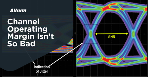
Improved power integrity also leads to improved signal integrity as shown in the eye diagram data below. In this graph, we can see that the eye diagram exhibits significant jitter, even when we use thin FR4 as the power/ground plane pair laminate and 100 SMD capacitors to support low PDN impedance. This occurs because ripple on the PDN will also cause variations in the signal level when an output buffer circuit switches logic states. The result is variation in the timing of the output signal, which appears as jitter in the eye diagram.
The graph on the right shows an eye diagram with an ECM and no SMD capacitors in the test board. The result is approximately factor 2 reduction in jitter and a larger eye opening. This is a clear improvement in signal integrity and it resulted entirely from reducing ripple on the power bus.
The above factors illustrate the well-known relationship between SI and PI. There is also a reduction in radiated EMI measured from the edges of the PCB when ECM materials are used. This arises because radiation generated by power bus ripple will experience greater dielectric damping as it travels to the board edge, thus it will leave the board with lower intensity.
Where to Use ECMs
Not all PCBs will need to use an ECM to provide power integrity. In some cases, the level of capacitance provided by an ECM is overkill, and you will be able to provide enough capacitance in your PDN with standard laminate materials and small-case capacitors. In some designs, an ECM that is very thin is one of the only solutions that will provide the required capacitance needed for power integrity. Some of the typical instances where ECMs are used in a PCB include:
- Small boards that support a lot of high speed signals (mobile devices, tablets, etc.)
- Low layer count boards with many high speed buses (advanced IoT products and mmWave sensors)
- Very dense, moderately small boards that do not have room for discrete capacitors (older phones, newer expansion cards, small motherboards)
Lower layer count boards (6-10 layers) will tend to use an ECM in the central layer between a dedicated power layer and a ground plane. In higher layer count boards (up to possibly 24 or 32 layers), the layer pair assignment can vary, but a very thin layer will be needed to provide sufficient capacitance to support SI/PI for all signals in the device. The same strategy is used for IC substrates.
PCB ECM Properties
A list of possible material properties for ECM materials for use in PCBs is shown in the table below. These materials are available as rigid materials (e.g., FaradFlex and 3M), or they can be incorporated on flexible polyimide materials (e.g., from DuPont). They are engineered to be incorporated into a standard lamination process for building a PCB stackup.
|
|
|
|
|
|
|
|
|
|
|
|
|
|
|
|
|
|
|
|
|
|
|
|
|
|
|
|
|
|
|
|
Package and Module ECMs
ECMs are also marketed for use in IC substrate packages. These packages involve placing a semiconductor die onto an organic substrate, possibly sitting on an interposer to provide additional connectivity between the semiconductor dies, the package substrate, and eventually the PCB. The substrate material then fans out those copper connections to the package’s BGA pattern on the bottom side of the package.
For packages and modules, layer thickness is also much thinner than the typical FR4 laminate, but with a target Dk value that is much higher than the materials used in a PCB substrate.
|
|
|
|
|
|
|
|
|
|
|
|
|
|
|
|
|
|
|
|
|
|
|
|
It’s important to note that an ECM that is marketed for a PCB could also be used in an IC substrate, but it would not necessarily be as effective. Note that some ECM materials are marketed specifically for PCBs or ICs (for example, FaradFlex). In contrast, some ECM product lines (such as 3M) are marketed for use in both PCBs and ICs.
In general, ECMs for use in IC packaging have the following requirements:
- Higher Dk value is preferred
- Higher loss tangent is preferred
- Thinner layer thickness is preferred
- Tg value is less important
The higher Dk value is a requirement because we would like to have larger plane capacitance density (measured in capacitance/(substrate area)). The Tg value is less important because the Tg values for ECM materials are already well above the temperature limits for ICs. The higher loss tangent in an ECM (both for PCBs and for IC substrates) is important for controlling ripple and will be discussed more in one of the sections below.
In order to provide the same capacitance as a lower Dk ECM in a PCB, the ECM used in an IC substrate would have to have much higher Dk because the size of the package substrate will be smaller. This gives an IC substrake sufficient package capacitance that aids on-die power integrity in the GHz range, particularly when the package does not have room for chip capacitors and there is little on-die capacitance. Because a PCB tends to have a larger area, they can get away with a lower Dk value if needed.
ECM Layers in Your CAD Tools
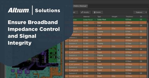
Incorporating an ECM into your PCB stackup inside your CAD tools is simple. You just need to define the material properties and thickness in your PCB stackup, just like you would with any other material. If you plan to use your board in a field solver simulation, such as for power or signal integrity, then you will need to include the dielectric properties in your layer stackup definition so that these can be considered in a simulation model.
It is also a good idea to define your material choice in your PCB stackup on your fabrication drawing and in a fabrication note. When you create the stackup figure in your fabrication drawing, make sure the ECM layer is present and that it will not be confused for an FR4-grade material or some other material. If you use Draftsman, you can generate your layer stackup figure automatically and quickly place this into your fabrication drawing.
Also, make sure your ECM specification is called out in your fabrication notes. The IPC standards conformance of your ECM, the thickness, copper weight, layer pair, distributor part number (if available), and brand name should all be specified in a fabrication note. An example is shown below.

As electronics continue to push the limits of feature density and component density, ECMs will be more important for ensuring sufficient decoupling when space for discrete capacitors is limited. Similarly, for IC packages incorporating multiple dies in 2.5D and 3D, sufficient decoupling is needed to ensure in-package power integrity when on-die capacitance is low. To learn more about the usage of these materials in PCBs and substrate packages, I encourage readers to access the following resources.
- Novak, Istvan.“SUN’s Experience with Thin and Ultra-Thin Laminates for Power Distribution Applications,” TechForum TF-THA2, DesignCon (2006).
- Borland, Bill. “Decoupling of High-Performance Semiconductors Using Embedded Capacitor Technology,” 2006 15th IEEE International Symposium on the Applications of Ferroelectrics.
Whenever you need to specify materials in a layer stackup for advanced high-speed digital PCBs and IC packages, use the complete set of product design tools in Altium Designer®. The Layer Stack Manager gives you full control over your PCB stackup, including material selection and impedance calculations. When you’ve finished your design, and you want to release files to your manufacturer, the Altium 365™ platform makes it easy to collaborate and share your projects.
We have only scratched the surface of what’s possible with Altium Designer on Altium 365. Start your free trial of Altium Designer + Altium 365 today.


