


PCB Debugging: Tips, Tools, and Tricks

At a Glance
There are some basic testing and PCB debugging steps you should take when your new prototype has some functionality and signal integrity problems.


It every designer’s nightmare: you receive boards from your prototyping run, you power them up, and you suddenly find nothing works as expected. Even worse is a critical failure that causes a short, creating a beautiful plume of blue smoke and the familiar smell of burning plastics and resins. Where do you start when trying to locate problems in your new board? What tools do you need to investigate different types of failure? There isn’t always a clear answer.
Different types of devices will require different debugging steps, so we can't generalize to everything. If you need to debug a new board and are unsure where to start, we’ve got some tips to help you get started and the important tools you’ll need to identify problems in your board.
PCB Debugging Starts By Isolating the Problem
The first step in debugging is to isolate the problem area in your board. When you test a new board, the first thing you probably look at is the easiest-to-test functionality: does the device provide the functions it was designed to provide? This could be reframed to be something as simple as "does the device turn on?" to "does my flashing application recognize my processor?"
This often involves tracing backwards within a functional block from the user interface or outputs and testing each component or interconnect in the suspected signal/power chain. Sometimes, the component that appears to have failed or be incorrectly placed is not the actual component that has failed, the real problem may be somewhere else in the board, and it's up to you to determine this. Some of the most common failures appear in the following ways:
- Opens and/or shorts: Assuming the board was fabricated correctly and passed any continuity tests, the problem could be linked to a specific component or group of components. In my experience, anytime I've seen this happen it is as simple as the wrong resistor, a very slightly lifted component, or a failed connection due to an incorrect footprint.
- Excessive noise: This comes in many forms and requires more investigation, but there are a few areas you can probe to at least narrow down the problem to a specific component, or even a specific I/O. In some cases, you can trace the problem back to a problem in the layout or routing, and this can be solved in your next board spin.
- Excessive heat: This can be as simple as a correctly functioning board where heat generation was not sufficiently considered during design time. This one is much easier to pinpoint
- Unexpected logical functions: This problem, while easily reproduced, is often one that requires a very detailed look at your datasheets, program logic, and connections between your host controller and all peripherals.
The point to all of this is: simply stating the device "is not working" is not a sufficient diagnosis. You need to identify the specific problem. In what follows, I'll assume the board has been fabricated correctly, and fabrication matches the design outputs as verified during in-circuit testing. Take a look at this article from Mark Harris for a full list of equipment you’ll need in any electronics lab, I'll mention some of those tools in the following sections.
Testing Opens and Shorts With a Multimeter
In the case where a specific component or small group of components appears to have failed completely, the problem may be as simple as a short circuit or open. This could be from an assembly defect or simple a failed component. Depending on where you went for assembly, you might not have received the level of service needed to ensure your board was assembled with best DFA practices. The best manufacturers will perform a thorough DFM/DFA review to ensure your design can be produced with very low probability of defects.

You’ll need to test for a short circuit or open circuit in the relevant section of your board. The cheapest tool you can get to do this is a decent multimeter. It doesn't need to be fancy, it just needs to be able to measure down to mV voltage and mA currents. Most home improvement stores will sell reasonably-priced multimeters that you can use to probe your board and check for opens and shorts. To check for failed or lifted connections at solder pads, measure the resistance between a component lead and its exposed pad; you'll measure an overload resistance if there is an open. Similarly, measure across neighboring pads to check for a short; you should measure non-zero resistance if there is no short.
Once an open is identified where you expected an open, it's pretty easy to check whether it is causing your problems. Simply bridge the two nodes where you see the open with a wire, and test again to see if the design will operate correctly. This is simpler when you can probe a via or pad directly, and this is one justification for leaving your vias un-tented. The same idea is not so easy with short circuits as it might require physically cutting the problem line, which will not be possible if the affected trace is buried in the layer stack.
If you have a BGA component, and the footprint is incorrect, the component can still solder to the board, but it will create open and short circuits throughout the footprint. Any vias used to make connections to the component along the routing path could be used to probe opens and shorts, and this may explain why you are not seeing what you expected, even though the board appeared to pass through fabrication and assembly correctly.

Excessive Heat
When heat is the issue, you can almost always isolate it to a specific component. Something as simple as your finger can be used to identify the hottest component in the board. If the component is very small or board space is cramped, you can also use a small thermometer. Simply probe around different components and you'll eventually find the culprit. If you want to get fancy, or you want to get a visual readout as to how heat is moving around the board, grab a thermal imager! These days, you can get a decent thermal camera for about $100 online.
The quick-and-dirty way to test for heat problem that might be created by a short circuit that is passing high current and creating heat is to use a can of nonflammable aerosol freeze-it spray or compressed air (take a look at this video for a demo). These cans are cheap and can be ordered online. You can spray the aerosol in the suspected area and power up the board; if there is a short circuit, the portion with the short will heat up quickly, and the aerosol will evaporate from this section of the board first. This helps you narrow down to the specific region or even the specific component that is involved in the short circuit.

In newer, more advanced devices, thermal management is still important, particularly when you start playing with mmWave devices. Ultra-high speed devices are the poster children for high heat generation by planar components, but power system components and RF amplifiers are the two other big heat generators in advanced devices. In some cases, one of these devices may power on successfully and operate for some time in the lab. However, once critical components heat up to high temperature, they may shut off or fail completely during operation. Keeping an infrared thermal imager around and monitoring temperature during testing can help you identify when a component or module gets too hot and shuts down. This has been a known problem in newer 5G handsets, although more advanced semiconductor materials (GaAs, GaN, GaN-SiC, etc.) used in microwave ICs are more resilient and can withstand overheating. Once you’ve identified the specific problem, you can investigate changes to your thermal management strategy.
Near-field and High-bandwidth Probes for Noise/Signal Measurements
Once you’ve isolated the particular component in a functional block that is failing, and your design has passed an opens and shorts test, the problem may be one of noise relating to signal integrity, power integrity, and EMI. On signal lines, EMI/SI problems can cause an IC to trigger at the incorrect times, creating incorrect outputs or causing a component to appear to fail altogether. On power nets, noise can cause an IC to glitch due to excessive power fluctuations. In the event core voltages drop too low, the device momentarily powers off and has to reset, basically failing momentarily and coming back online in the middle of executing instructions. The other SI/PI problem that needs debugging is ground bounce, which represents an intersection between SI and PI.
In the absence of any test structures on your board, you’ll need to measure signal behavior throughout your interconnects. A near-field probe is useful for capturing a signal measurement in the time domain with an oscilloscope. The alternative is to use a direct high-bandwidth probe to get the same measurement with an oscilloscope. Just be mindful of your oscilloscope bandwidth if you need to example high speed interconnects and the possibility of very fine signal distortion in the time domain in impedance controlled traces. The frequency content can then be examined with a signal analyzer, using an FFT in software. Newer near-field probes and commercial high-bandwidth probes have bandwidths reaching multiple GHz, making them useful for many high speed and high frequency devices.

Power Integrity Diagnosis
If you’ve eliminated signal distortion, skew, and impedance problems from your board, and your components are still not triggering correctly, you may have a power integrity problem. This arises in two forms:
- High PDN impedance leads to ringing on power connections, which then leads to excessive jitter and distortion on the output from a component.
- Switching noise from a power supply could also be the culprit, although this problem normally appears at much lower frequency than PDN ringing.
In this case, you’ll need to examine power stability on any power rails, on the power supply output, and at any bypassing/ground connections. You'll want to do this while the device operates with the probes listed above. Commercial probes can measure low-level power disturbances created by components with high I/O count switching at high speed. If the problem is noticeable when the device is switching, the problem might be due to power rail collapse, ground bounce, or both.
All of these problems are linked to high PDN impedance on the board, something which might be solved with something as simple as increased decoupling (more capacitance). Verifying this involves some complex mathematics, where you invert the current and voltage waveforms back into a PDN impedance spectrum using convolutions and/or FFTs. However, you can verify whether insufficient decoupling is the culprit by soldering additional decoupling capacitors on top of each other. This puts them in parallel and allows you to experiment with the amount of capacitance on your PDN.
Other Specialized Tests
The problem with an assembled board that is failing due to noise is that it can't be easily debugged in the same way you would play with opens, shorts, and heating. You can't really check the fundamental metrics like impedance and propagation directly, so you have to infer things like signal reflections, losses, skew, and distortion from the above signal measurements. If you expect one of these issues to be a problem, you should at least request controlled impedance testing from your manufacturer, or you should plan ahead with test fixtures so that you can take direct measurements.
There are some other signal measurement techniques that can be used to determine whether signals are being significantly distorted along an interconnect. Read more about test structures you can include for different interconnects:
- PCB Design For Test—Test Structures And Types Of Tests, Part 1
- PCB Design For Test Structures And Tests Performed, Part 2
- Validation Structures for Signal Integrity
Embedded Debugging
In the case of an embedded system or a device that must interface with a computer, you may be looking at problematic results on a computer screen. Bringing software into the mix complicates things significantly, as the problem may lie within the software rather than the board itself. Any firmware/software involved in a new product should be tested separately from the board in order to ensure there are no errors in the code. When software is tested on its own, you can initially isolate logical errors before flashing and testing the PCBA.
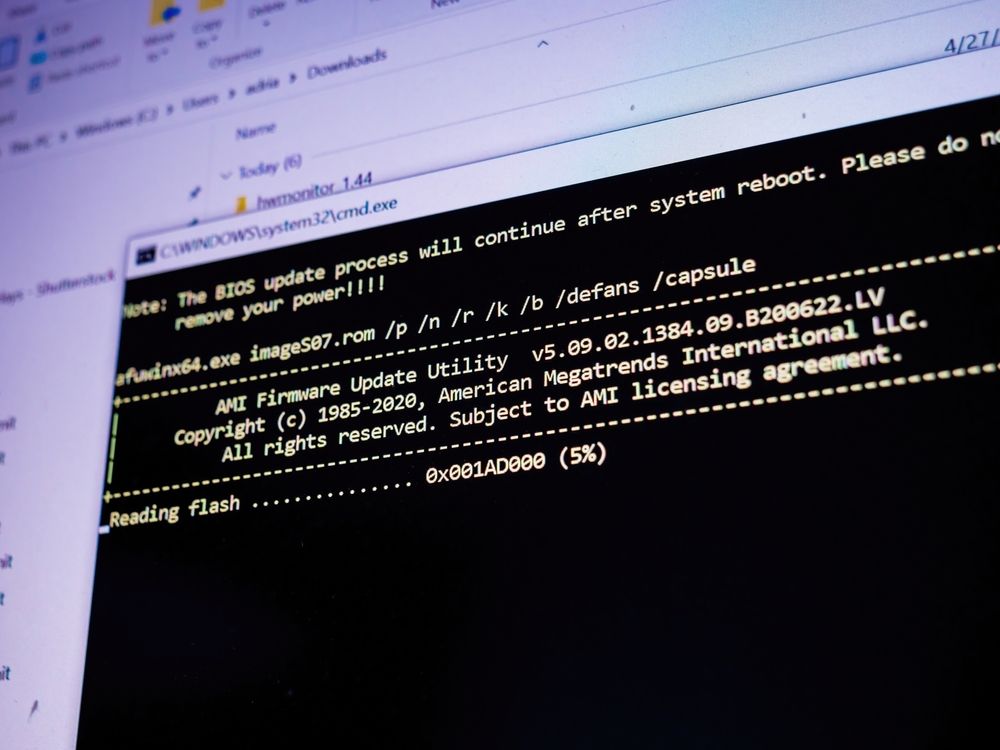
Once you flash firmware onto the board or boot from an image, you might find other problems that were not evident in other sets of tests. Even if the code appeared to be written perfectly, functional errors could indicate a hardware design problem or a logical problem. If you're doing anything with embedded, I would start by flashing the board after doing an initial power-on test and check that the main functional blocks receive power in standby mode. Then I would flash the code and start doing functional testing and debugging. Throughout the process, if you see functional errors during testing and you've eliminated any hardware problems, it's time to go back to your code and verify it was written correctly.
Long-term PCBA Testing and Redesigns
Certain boards will have their own long-term reliability concerns that need to be investigated. Depending on your application and deployment environment, long-term testing of the PCBA may not be appropriate or needed. For high-reliability products, you might consider an initial round of environmental tests with your prototype, where the PCBA is stressed to its limit. In these products, where long-term continuous operation is required, these extensive tests are an important part of debugging not found in most general-use electronics.
The pre-layout and post-layout analysis tools in Altium Designer® can be a big help in PCB debugging as you can easily implement design changes and verify these with your team or manufacturer. When you’ve finished your design, and you want to release files to your manufacturer, the Altium 365™ platform makes it easy to collaborate and share your projects.
We have only scratched the surface of what’s possible with Altium Designer on Altium 365. Start your free trial of Altium Designer + Altium 365 today.

About Author
Related Resources
Table of Contents
Design to Release, Without the Friction
- Keep reviews tied to the right version
- Reduce handoff confusion and rework
- Spot sourcing and release risk earlier
- Work solo, share when needed
Get Started
Thank you, you are now subscribed to updates.


