


PCB Design Variants: Managing Multiple PCBA Versions

At a Glance
Manage each variant of your PCB design in a single platform, without complicated sheets, folder structures, or multiple PLM entries.


It is often the case that a PCB project needs a mix of component installations, part numbers, and paste settings, even with the same layout and schematic design. PCB project variants are created to control these settings during development and production. It then becomes a design team's responsibility to keep track of what is in each variant and why that variant was created, as well as the purpose of the assembly variant.
In development, the most common requirement is control over DNI settings in the PCB assembly, which needs to be notated in the schematics and in the BOM. In the classic approach to variance, this involves creating multiple assembly packages and manually notating outputs so that each variant could be built and assembled. This has historically been a time-consuming process that produces a large number of file sets, each requiring their own tracking and documentation.
See how you can easily manage variants inside your ECAD software and eliminate the huge numbers of files for each project in this article.
What Changes in Each PCB Variant?
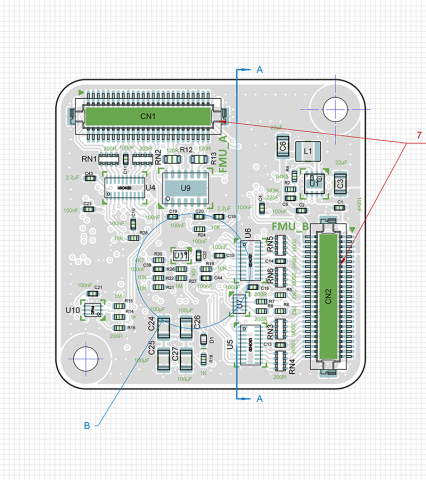
PCB variants are very useful for tracking slight differences in PCB layout and schematics for a single project. Once a schematic design is locked in and a PCB layout is complete, the designer modifies various aspects of the design to create a variant.
- Component installation status (Fitted or Not Fitted)
- Alternate part numbers assigned at the component level
- Component parameter values, such as resistance or capacitance
- Alternate footprints for specific components
- Solder paste mask settings per assembly configuration
- Jumper and zero-Ohm resistor population for hardware configuration control
Once the variant is specified, unique PCB design outputs are generated for each variant. Individual variants can be used for separate fabrication and assembly jobs as needed.
Common Use Cases for Variants
The most common instances where variant PCB designs are used heavily are in early prototyping and in volume production. Low-rate production, such as an initial production run, does not rely on variants as often as the other two cases.
Prototyping Variants
During prototyping, PCB design variants give engineers a structured way to test multiple configurations from a single board build. Configuration pins on ICs are a typical target: rather than cutting traces or bodging resistors, a designer creates separate variants with specific pull-up or pull-down resistors marked DNI, enabling trial-and-error configuration testing in an organized and repeatable way.
In prototyping, the usage of DNI designations primarily impacts the information in the BOM, where certain lines are labeled "Fitted" or "Not Fitted" to denote which parts are DNI. This is the easiest way to set up a BOM so that the assembly instructions are accurately reflected and easily readable.

Fitted/Not Fitted components can be viewed visually in the schematic and included in the BOM for the PCB variant.
Production Variants
In volume production, PCB design variants are most commonly used to manage alternate part numbers and alternate footprints rather than DNI configurations. When a preferred component becomes unavailable or a qualified replacement carries a slightly different land pattern, defining a production variant allows the engineering team to formalize the substitution within the design database rather than issuing informal deviation paperwork. This practice keeps alternate configurations traceable and ensures that each production build is tied to a specific, documented variant with its own output package.
This usage of variance allows some agility during production in order to address supply chain disruptions and quality control problems. It is often the case that during production, a particular part may go out of stock or a footprint needs to be modified (for example, from LMC to MMC in SMD passives) to eliminate an assembly defect. Switching to a new variant allows changes to be implemented quickly and without major changes to the design files.

In this case, an entirely unique PCB design outputs package will need to be generated for the design database for each variant. This is because the fabrication data is also often modified when defining the variant, as in the case of footprint changes. Other pieces of documentation may need to be modified as well, such as fabrication and assembly notes in master drawings.
Best PCB Design Software For Managing Variants
Variant management is a relatively new feature that has been fully implemented inside of Altium Designer, the industry's most popular and most capable PCB design software platform. Users can create and edit design variants at any stage of the product lifecycle, and by leveraging the templatized output generation tool in OutJob files, users can instantly generate complete manufacturing file packages for a PCB design variant.
Setting Up Variants in Altium Designer
Variant setup in Altium Designer is managed through the Variant Management dialog and requires only a few steps to configure correctly. The process follows a consistent sequence regardless of whether the variant is intended for prototyping or production.
- Open the project and navigate to Project > Variants to access the Variant Management dialog.
- Create a new variant and assign it a unique, descriptive name that reflects its purpose or configuration state.
- Select individual components and assign installation status (Fitted or Not Fitted), alternate part numbers, or alternate footprints at the component level.
- Verify that the schematic and BOM reflect the correct variant parameters before generating outputs.
- Use an OutJob file to generate a complete, variant-specific output package including Gerbers, assembly drawings, and the BOM in a single operation.
This workflow keeps all variant definitions inside the project file rather than scattered across external spreadsheets or folder structures, which significantly reduces the documentation overhead that comes with managing multiple board configurations across a product development cycle.
Whether you need to build reliable power electronics or advanced digital systems, use Altium’s complete set of PCB design features and world-class CAD tools. Altium provides the world’s premier electronic product development platform, complete with the industry’s best PCB design tools and cross-disciplinary collaboration features for advanced design teams. Contact an expert at Altium today!
About Author
Related Resources
Related Technical Documentation
Table of Contents
Design to Release, Without the Friction
- Keep reviews tied to the right version
- Reduce handoff confusion and rework
- Spot sourcing and release risk earlier
- Work solo, share when needed
Get Started
Thank you, you are now subscribed to updates.


