







PCB Assembly Outputs

At a Glance
Learn about the important PCB assembly output files. Manufacturers use these to source components, understand process requirements, and assemble the PCBA.


When you complete a PCB design, the intent is normally to have it manufactured and assembled. It is the designer's responsibility to prepare PCB assembly outputs with the project and supply them to the manufacturer. The manufacturer will use these outputs to procure parts, plan the assembly process, and perform a final inspection. The assembly requirements should be detailed, giving the assembler the comprehensive information required to complete a PCBA build.
Before you get to assembly, your board has to be designed with best DFA practices implemented. If it is not, and the PCBs are fabricated before review by an assembler, there is a risk that the PCBs will have to be scrapped. There are many reasons why scrapping occurs, but the right ECAD software for PCB design will help designers avoid some of the most common assembly mistakes.
List of PCB Assembly Outputs
At the most basic level, the two standard PCB assembly output files are the bill of materials and a pick-and-place file. The bill of materials is a purchasing document that specifies which part corresponds to each reference designator on the PCB, and the pick-and-place file states where each reference designator is to be placed for soldering. With these two files and a brief description of the PCB, or no description at all, a manufacturer can fully assemble a PCBA.
Professionals and companies generally create a third standard design output: an assembly drawing. An assembly drawing typically contains:
- The PCB outline and board dimensions
- Top-side and bottom-side component outlines
- Component reference designators
- Component polarity and orientation indicators
- Pin 1 indicators for integrated circuits and connectors
- Mechanical hardware and mounting locations
- Detail views for dense or complex areas
- Assembly notes, callouts, and special manufacturing instructions
- Revision information, drawing numbers, and title block information
Assembly notes are important because they define requirements that may not be obvious from the PCB layout, bill of materials, or pick-and-place data. These notes can specify RoHS compliance, conformance with applicable IPC standards, the use of specific solder alloys or solder paste types, cleaning requirements, inspection criteria, and special processes such as underfill, conformal coating, staking, or adhesive application. Clear assembly notes reduce ambiguity and help ensure that the finished PCBA meets the designer's mechanical, electrical, and regulatory requirements.
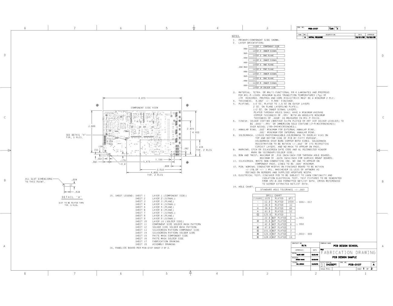
Many new designers do not create assembly drawings because their CAD software does not help automate the process. Even some enterprise software, such as OrCAD and Xpedition, does not have the ability to create an assembly drawing automatically. These platforms may rely on other software with a separate license to perform this fundamental task.
Altium Designer is different because it includes the Draftsman tool, which allows designers to automatically create high-quality assembly drawings in minutes. Users can create custom templates and sheet sizes that provide full control over the format of an assembly drawing. Users can also place additional features in an assembly drawing, such as embedding the BOM, adding notes and callouts, and embedding project parameters for instant drawing updates.

If you are not a fan of using the tool to generate a fabrication or assembly drawing, there is still a way to create these drawings inside a PCB layout file. One common practice is to use the mechanical layers in your PCB layout to draw the fabrication and assembly drawing features by hand. This way, updates to the PCB layout are also immediately reflected in your assembly drawing. To output the assembly drawing, you would need to compile the following layers into a DXF file or PDF print:
- Mechanical layers with the title block and assembly notes
- PCB outline layer
- Top and bottom paste mask layers
- Top and bottom assembly layers
- Any additional mechanical layers showing peelable mask, conformal coating, adhesive locations, and other special assembly requirements
It is also common to include isometric views of the PCB generated from a 3D drawing. However, mechanical layers and PCB layout tools cannot normally generate isometric views, so they need to be created in an external MCAD application from a 3D model of the PCBA. The view would normally be exported as a DXF file from the MCAD application and imported back into the PCB layout file on a mechanical layer. However, Altium Draftsman can generate isometric views directly from the PCB document file without requiring export to an MCAD application.
Intelligent PCB Design Outputs
Another option for creating PCB design outputs for assembly is to use intelligent output formats. These file formats are ODB++ and IPC-2581.
| ODB++ | IPC-2581 |
|---|---|
|
|
Although intelligent PCB design outputs are objectively better for fabrication and assembly, they are not used as often as Gerber files. Gerbers still remain the de facto standard for fabrication data, so a designer will also have to output a bill of materials and pick-and-place data for assembly. To make sure you have the broadest range of PCB assembly options, use PCB design software such as Altium Designer, which supports all three standard PCB design output packages.
Successful DFA Prevents PCB Assembly Defects
When assembling PCB prototypes, the vendor's service level typically includes enough margin to account for rework of your PCB as needed. However, as you scale to higher volumes, preventing defects and avoiding required rework become critical parts of cost control. DFA practices become even more important at this stage, and they relate to basic design practices that occur in the PCB layout and PCB libraries.
To successfully implement DFA practices for high-yield PCB assembly, designers need to leverage their ECAD software and information from their assembler as follows:
- PCB component footprint design
- Defining assembly constraints as PCB design rules
- Examining the PCB in an assembly review
PCB Footprint Design in DFA
Footprint geometry is where DFA either succeeds or breaks down at the component level. A footprint that does not match the assembler's process capabilities introduces defect risk regardless of how well the rest of the layout is executed. Pad dimensions, courtyard clearances, solder mask openings, and land pattern geometry all feed directly into placement accuracy, solder joint formation, and post-reflow inspection access.
For standard SMD packages, IPC-7351 provides a baseline, but the assembler's specific process, whether wave, reflow, or selective solder, will determine which land pattern variant is appropriate. Using the nominal or most-courtyard land pattern when the assembler runs a high-density profile, for example, is a common mismatch that produces bridging or insufficient heel fillets.
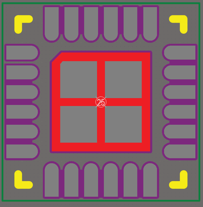
This footprint is designed to implement DFA best practices on soldering the central pad in order to prevent solder wicking and shifting during soldering.
PCB Design Rules For DFA
To ensure consistent DFA, enforce guidelines through automated design rules rather than manual inspection. Obtain specific constraint values directly from your PCB assembler, e.g., component spacing, paste aperture ratios, and tolerances. Do not rely on generic IPC defaults, as they may not align with your assembler's capabilities, especially for fine-pitch components.
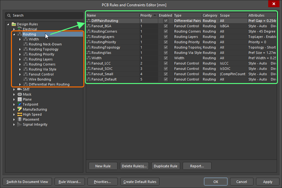
Apply assembler-supplied constraints directly into your PCB software's design rule system to prevent assembly defects. This includes defining rules for component courtyard clearance, paste mask expansion, and solder mask registration, ensuring the design rule check catches potential issues before fabrication.
- Minimum component-to-component courtyard clearance, sourced from assembler capabilities documentation
- Solder mask expansion per pad type, distinguishing SMD from NSMD pad definitions
- Paste aperture area ratio minimums, typically 0.66 or higher for reliable paste release
- Pick-and-place keepout boundaries near board edges and tooling holes
- Via-in-pad rules for thermal pad patterns, including tenting or filling requirements
Inside Altium Designer, any of these constraints can be implemented using the PCB Design Rules and Constraints Editor, or using the newer Constraint Manager. Users of platforms like Cadence OrCAD/Allegro and Siemens PADS/Xpedition will be more familiar with the Constraint Manager interface, which eases the transition to the more powerful design interface in Altium Designer.
PCB Assembly Review
The factors listed above are primarily implemented during the PCB layout phase and are made physical during assembly. Unfortunately, if you do not get an assembly review before fabrication, it is possible that a sub-optimal PCB is produced which does not fully align with DFA capabilities. In simpler boards with large-case SMD components or large through-holes, this may be a non-issue. But in dense PCBs, HDI PCBs, or flex/rigid-flex PCBs, failing to follow assembler constraints is likely to lead to defects in the PCB assembly.
For this reason, designers should consider sending their fabrication data to a PCB assembler for review. This can help identify simple design issues that will lead to defects, and these can be corrected before the bare boards are fabricated. If this is not done, particularly when producing at volume, be prepared for defects, rework, and even scrapped PCBs.
To learn more about PCB assembly outputs as part of a comprehensive manufacturing package, watch the video below.
Whether you need to build reliable power electronics or advanced digital systems, use Altium’s complete set of PCB design features and world-class CAD tools. Altium provides the world’s premier electronic product development platform, complete with the industry’s best PCB design tools and cross-disciplinary collaboration features for advanced design teams. Contact an expert at Altium today!
Frequently Asked Questions
What files are required for PCB assembly?
The minimum PCB assembly package includes a bill of materials and a pick-and-place file. Professional manufacturing packages should also include an assembly drawing with component locations, orientation indicators, mechanical details, revision information, and assembly notes.
What information should be included in a PCB assembly drawing?
A PCB assembly drawing should show the board outline, dimensions, component outlines, reference designators, polarity markings, pin 1 indicators, mounting hardware, and detail views. It should also include assembly notes, special process requirements, drawing numbers, and revision information.
How do you create a PCB assembly drawing in Altium Designer?
In Altium Designer, designers can use Draftsman to automatically generate assembly views from the PCB document. Draftsman also supports custom templates, BOM tables, notes, callouts, project parameters, and isometric board views.
What is the difference between ODB++ and IPC-2581?
ODB++ is a proprietary intelligent PCB data format, while IPC-2581 is an open, vendor-neutral IPC standard based on structured XML. Both can combine fabrication, assembly, component, connectivity, stackup, test, and inspection data into a single manufacturing package.

About Author
Related Resources
Related Technical Documentation
Table of Contents
Solutions for Every Role and Team
- Discover and evaluate design options earlier
- Develop in one shared workspace
- Scale with control and compliance
- Connect every stage of hardware development
Learn More
Thank you, you are now subscribed to updates.



