How to Build a PCB Footprint Library With Altium

Many components come in standardized packages, but not all component manufacturers provide CAD models and schematic symbols in their PCB libraries. These CAD models show the location of pins, silkscreen information, centroids, and pads as they should appear in your PCB layout. PCB component creation can get repetitive when you need to apply an existing PCB footprint to a new component.
With Altium's component creation tools, you can quickly create PCB component libraries, including OCB footprint libraries, to reuse existing component data in new components. You won’t have to repeatedly import data when you’re generating component variants, and you can instantly make this data accessible to anyone on your design team.
Most design tools don’t make component reuse easy. But when you use Altium, you won’t need to go through a repetitive download and upload process to apply an existing PCB footprint to a new component. You will be able to select pre-made footprints from a centralized PCB footprint library. Many components have multiple variants, often with the same package and pinout. If you’re a component manufacturer creating parts models for your customers, or you’re a board house and you can’t find the model you need, reusing existing CAD models for your components greatly cuts down on the time required to create libraries. If you want to quickly reuse components, you can do all of these tasks and more in Altium.
PCB Footprint Creation and Reuse in the Cloud
The old way of reusing components required manually copying data between libraries in PCB footprints and schematic symbols. The compiled libraries would then need to be shared via email, a proprietary management tool, or looked up in a database. Altium's PCB library management stores your shared components in a secure cloud environment. You can regulate access to different components and projects with Altium's granular access permissions.
Getting Started with PCB Footprint Creation and Reuse
Once you’ve logged into Altium, you can bring up the Altium Explorer window and create your PCB footprints and schematic symbols. To get started with PCB footprint reuse, create a new part. You’ll see the window below, which allows you to create a schematic symbol, PCB footprint, and SPICE simulation model.
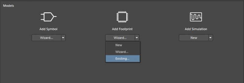
Creating a new component in Altium. You can use the standard IPC-compliant component generation Wizard, or you can reuse an existing component from your Altium repository.
Even if you’re creating component variants with identical pinouts, you’ll likely need to apply some customization to your schematic symbols. However, as a PCB footprint is a 2D representation of your PCB component, it’s more likely that you can reuse an existing component with little or no modifications.
After selecting “Existing” from the dropdown menu in the window shown above, you’ll be able to scroll through your existing PCB component library for footprints. You can also search by keyword, electrical specification, footprint name, or component type. Simply locate the PCB footprint you want to use from your existing library and search results.
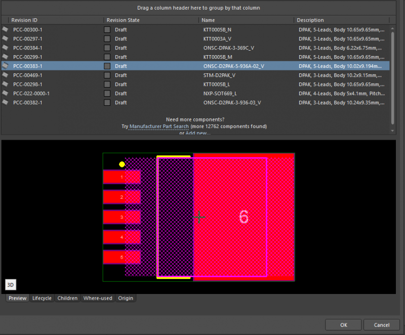
Searching for a DPAK component model using the Altium Explorer window in Altium.
If there is a 3D CAD model (e.g., from a STEP file) that is attached to the existing component, it will also be assigned to your new component. The image below shows the 3D CAD model for the DPAK component shown above in the Altium 365 Explorer window. All this data was accessed with only a few clicks, without downloading any files, and without importing and exporting libraries between programs.
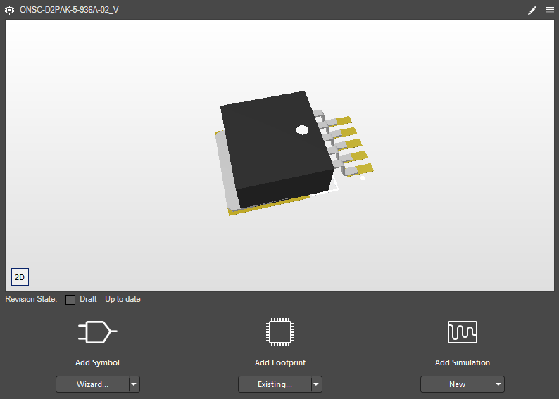
3D model for a DPAK component in the Altium Explorer window in Altium.
Once you’ve created a new component from an existing footprint, you can quickly import your simulation file and create a schematic symbol for the new component. For the schematic symbol, you can also access the symbol creation Wizard. After you’ve finished entering all your component specifications and description for the new component, you can easily push it to your cloud PCB component library in the Project's panel. This is by far the easiest way to reuse PCB footprint data and share it with your design team.
- With the right design tools and data repository, you can easily reuse other design documents to decrease your PCB design time. Learn more about strategies for reusing PCB design data in new projects.
Simplify Component Data Access and Reuse
Placing your important component data on the cloud accelerates electronic product development by making access and reuse extremely easy, but other collaboration platforms simply can’t provide the required level of integration. Altium simplifies these data-sharing and component management activities thanks to its secure and centralized cloud collaboration.
Beyond Component Data Reuse with Altium
The features shown above only scratch the surface of what you can do with Altium. When you release a new project to your Altium cloud instance, other designers will have access to project data and the associated component and PCB footprint libraries. You can also synchronize fabrication outputs for a project without using a 3rd party cloud sharing platform. Whenever you import a component into Altium using the Manufacturer Part Search panel, it will be deployed to your cloud workspace as soon as you push your project.
- Altium includes a Manufacturer Part Search panel, which allows you to find verified footprints and symbols directly from manufacturers.
- Altium allows you to synchronize your project releases and fabrication data. Collaborating with your fabricator and assembler is much easier when you can quickly share and annotate your manufacturing data.
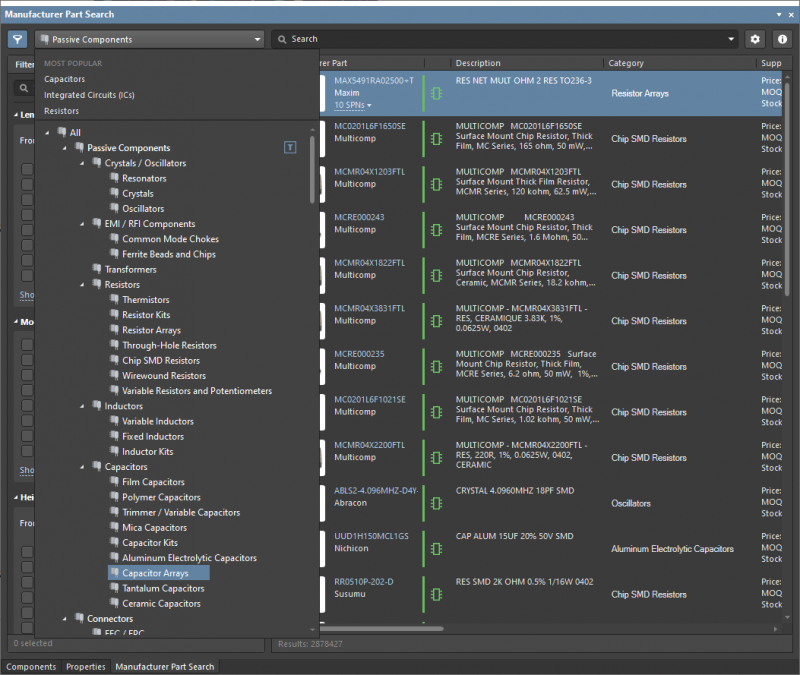
You access components with the Manufacturer Part Search panel in Altium.
Secure PCB Footprint Creation and Sharing in Altium
Your cloud tools are only easy to use when they are easy to access and integrate into your other important programs. There are plenty of data management tools on the market, but Altium is the easiest platform to integrate with other design tools. The ability to push and pull information through to the cloud makes makes your component and design data easy to access for authorized stakeholders.
Manage All Your Design Data with Altium
Altium doesn’t limit the management and sharing of your component data. You can store, share, and manage all your design data with Altium. Anyone with access to your Altium workspace can also access design data in Altium, and every revision to a design will be seamlessly tracked in the cloud. Altium provides this same type of integration with popular MCAD applications via seamless ECAD-MCAD collaboration. These systems finally integrate seamlessly, forming a complete product design suite.
- You can access a complete set of component and data management features in Altium. All this is accessible from Altium’s unified design environment.
Learn more about working in Altium’s integrated environment.
- Your project information will always remain secure when you use Altium. You can regulate access to important data from anywhere.
Altium is the ideal cloud platform for secure and collaborative electronics product development. Instead of separating component data management, access control, and design management features into separate applications, you can control and manage your designs in a single platform. If you’re ready to simplify component and footprint creation and streamline PCB library management, it’s time to try Altium.

