


Designing and Placing Silkscreen on your PCB with Altium Designer

At a Glance
Silkscreen on a PCB is just one important part of planning for manufacturing and assembly. Altium Designer makes it easy to place silkscreen on your next PCB.


Planning for the manufacturing and assembly of your next printed circuit board requires drafting a number of deliverables for your manufacturer. One of the important aspects of planning for assembly is ensuring that your assembler has the instructions they need to place components in the right locations and with the right orientation. When you use the right PCB editor with top-quality CAD tools, you can place silkscreen directly in your PCB layout and use a design rule check to verify appropriate clearances. Altium Designer gives you these tools and plenty of other features to help you prepare for manufacturing and assembly.
ALTIUM DESIGNER®
A unified PCB design package with the best CAD tools for PCB layout and silkscreen placement.
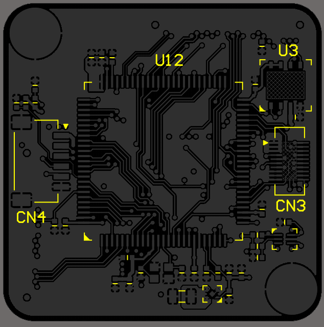
Silkscreen refers to a set of labels that are printed on the surface layers of a circuit board. Silkscreen includes each reference designator for your components, identifiers, company logos, switch settings, test points, part numbers, and any other information that an assembler needs to ensure they place the correct components in the correct locations. Silkscreen can also be useful for testing as a designer can put important safety notes, polarity indicators, or other information needed to quickly understand how a PCB operates.
If you’re designing a printed circuit board, your PCB design software will place important silkscreen information for you as long as your component data includes silkscreen information. Silkscreen communicates a significant amount of information required to properly assemble your board, and you should make sure this information appears in your component data so that it will be included in the PCB layout. Once you send the board in for manufacturing, they will need silkscreen layers for the top and bottom sides of the board. With the right CAD tools in your PCB editor, you can easily modify the location of silkscreen in your PCB layout without directly changing the component data. This is one of the final cleanup steps before planning for manufacturing.

Common Mistakes with PCB Silkscreen
Silkscreen is placed on the top and bottom overlay layers in order to distinguish it from copper layers or mechanical layers. Some of the common silkscreen mistakes include:
- Placing silkscreen too close to a trace; variance can cause the silkscreen to print directly on a copper element
- Placing silkscreen too close to a pad; if the silkscreen is printed directly on or near a pad, it can interfere with soldering
- Overlapping silkscreen for different components; this often happens when a design has a dense set of components on
- Ambiguous symbols, odd fonts, and small text; it's understandable that high density designs need smaller silkscreen, but it should be easy to read and understand
- Missing polarity or pin-1 indicator; the polarity and orientation, and first pin on an IC package should be clearly marked.
IPC standards require PCB manufacturers to place a manufacturer’s mark and a lot number using silkscreen. This allows a board to be traced throughout the supply chain in the event of a recall. Manufacturers generally place these marks away from critical areas, such as on the back side of a board or near the edge away from critical components. One common mistake is to neglect to tell your manufacturer where these markings should be placed on your board. Make sure to specify this if it should be kept away from specific areas.
Fabrication and Assembly Instructions
Aside from silkscreen and assembly instructions, your manufacturer will need a bill of materials that lists components that include reference designators. These reference designators must match your silkscreen in order to ensure that components are placed in the correct locations. This prevents unnecessary errors during assembly and makes your board easier to test and troubleshoot.
- Silkscreen is included on the top overlay layer in your ODB++ files or Gerbers. You’ll need to prepare a complete documentation package for your manufacturer, including overlay layers.
Learn more about creating manufacturing documentation. - Proper silkscreen placement in your PCB helps ensure that your manufacturer places your components in the correct locations and that important pads and test points are clearly indicated on your board.
Learn more about preventing manufacturing errors with proper silkscreen placement. - When creating models for proprietary components, the right design software will allow you to quickly add silkscreen information to your model, saving you time during layout.
Learn more about creating silkscreen for custom components.

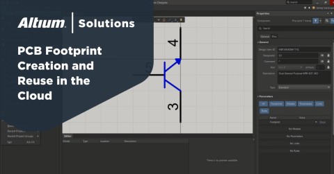
Creating IPC-compliant component footprints in Altium Designer. This tool will automatically place silkscreen on the top overlay layer.
How to Make Readable Silkscreen for Components in Altium Designer
When creating a new PCB footprint for a component, you can manually place silkscreen using the standard CAD tools in the component editor. If you know how to layout a PCB and use the standard drawing tools in the PCB component editor, you'll use the same tools to place silkscreen in a PCB footprint. To complete all the silkscreen you'll need for a component, you'll need to draw the component outline, pin-1 indicator (for integrated circuits), and reference designators. Some components may require additional silkscreen, such as polarity indicators. All of these elements are easy to place in Altium Designer's part library editor using the standard drawing tools and String tool.
Silkscreen Cleanup is Easy in the Best PCB Layout Software
After all the components are placed, there is often a need to cleanup silkscreen placement around your components. Sometimes, reference designators and outlines may overlap slightly, so it's not uncommon to need to adjust the positions of these elements in the layout. After cleaning up the silkscreen in your component data, you can place any other silkscreen information needed on the board. This can include a company logo, part number, UL/CE/FCC markings, and even environmental markings like RoHS.
- Checking silkscreen placement is one of many important DFM/DFA processes you should implement in order to decrease turnaround time and improve yield. Cleaning up silkscreen in the PCB layout is a common design requirement.
Learn more about DFM/DFA tips from expert Duane Benson. - Your reference designators can be quite large compared to other silkscreen elements in your PCB layout. It's a good idea to carefully place and arrange reference designators so that they do not interfere with each other.
Learn more about reference designators and how to place them in Altium Designer. - Getting started with PCB layout in a new program can seem complicated, but Altium Designer is here with a tutorial to help you get started.
Learn more about getting started with PCB layout in Altium Designer.
Use the viewing modes in Altium Designer to isolate silkscreen and cleanup your PCB layout.
Define Silkscreen Clearance as Design Rules for Accurate Fabrication
Silkscreen is just one important design element that helps ensure successful fabrication and assembly. Your silkscreen layer needs to have the proper clearances from your other design elements, and you can set the right clearances when you have the best PCB layout software.
Altium Designer's powerful PCB layout tools are built on a rules-driven design engine, giving you the power to take control over all aspects of a design through intuitive design rules. As you work through component placement and routing, Altium Designer's online DRC engine will automatically check the layout against standard and custom design rules to ensure the final design will function properly and is manufacturable. Altium Designer's complete toolset also integrates with production planning tools so you can create a complete manufacturing file package for your design in standard file formats.
Altium Designer: Unifying Design, Fabrication, and Assembly
With other PCB design platforms, your features are separated into different programs, and some important features required to properly place silkscreen may not be present in your design. Instead of risking your productivity and potential redesigns with other programs, Altium Designer gives you access to all the design and production planning features you need in a single program.
- Altium Designer includes all the layout, rules checking, and production planning features you need in a single environment. Your design features are unified on top of a single, rules-driven design engine, ensuring your designs and data remain error-free.
Learn more about rules-driven design in Altium Designer. - The power of Altium Designer is in its unified PCB design interface. Everything needed to design advanced electronics is available in a single program.
Learn more about the complete suite of PCB design tools in Altium Designer. - When you’ve completed your PCB layout, you can share your design data with other team members, your customers, or manufacturers through the Altium 365 platform. Altium Designer works together with Altium 365 so you can collaborate via a secure cloud environment.
Learn more about sharing your PCB design data with Altium 365.
Build the highest quality circuit boards with complete PCB silkscreen in Altium Designer.
There are plenty of design aspects to consider in any circuit board layout, and Altium Designer includes the tools you need to create the highest quality circuit boards in a single program. You’ll be able to operate at peak efficiency when you have access to design, production planning, verification, and data management features in a unified design environment. Don’t settle for other design platforms with separates features that force you to work between different programs. If you want to work with the best design and production features, then it’s time to make the switch to Altium Designer.
Altium Designer on Altium 365 delivers an unprecedented amount of integration to the electronics industry until now relegated to the world of software development, allowing designers to work from home and reach unprecedented levels of efficiency.
We have only scratched the surface of what is possible to do with Altium Designer on Altium 365. You can check the product page for a more in-depth feature description or one of the On-Demand Webinars.

About Author
Related Resources
Related Technical Documentation
Table of Contents
Design to Release, Without the Friction
- Keep reviews tied to the right version
- Reduce handoff confusion and rework
- Spot sourcing and release risk earlier
- Work solo, share when needed
Get Started
Thank you, you are now subscribed to updates.


