


How to Ensure Impedance Control in PCB Routing


Impedance control in PCB designs can refer to two different practices depending on who you're speaking with. PCB manufacturers provide impedance control as a service to customers who want to manufacture a high-speed digital system or an RF design. In contrast, PCB designers use the term to refer to intentional material selection and specification for their PCB stack-up, often without consideration of what materials a manufacturer might have available.
Whether you're approaching PCB impedance control from a manufacturing perspective or as a designer and want to ensure correct impedances are implemented in your board, your PCB design tool will play an important role. You'll need to use your stack-up construction tool or your drawing tool to specify the requirements for your build. These requirements will vary depending on who will be making the final material selection for your design.
While it is our view that PCB designers should take a more active role in selecting and specifying materials for their PCB stack-ups, there is value in taking the traditional controlled impedance approach and deferring to your manufacturer, especially in volume production. We'll explore these aspects of PCB impedance control in this article.
The PCB Manufacturer's Perspective
For PCB manufacturers, impedance control refers to the manufacturer selecting from their in-stock materials to build a PCB stack-up that provides specific impedance values. Essentially, the designer specifies trace geometry requirements, and the manufacturer selects materials that ensure the specified geometry has a target impedance. This reduces the burden on the PCB designer, as they do not need to make a final material selection.
Instead, PCB designers need to have some knowledge of each manufacturer's capabilities based on the PCB manufacturer's processing limits. As long as the trace geometry they select can be fabricated within the manufacturer's processing limits, it is likely to be a valid design where the manufacturer can support controlled impedance. The PCB designer needs to specify the following information:
- Trace width for single-ended signals
- Trace width and spacing for differential signals
- Routing layer for each of the above
- Desired impedance for each of the above
- Acceptable impedance tolerance
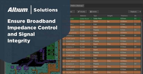
The most common way to specify this information is in a fabrication drawing using an impedance table or a transmission line table. For example, in Altium Draftsman, the trace parameters can be written into a small table and placed on the same page as the stack-up drawing.
An impedance table created in Altium Draftsman
Based on this information, the PCB manufacturer will mix and match their available materials to meet these impedance targets. They will then present this proposed stack-up to the customer for final approval. Although the manufacturer will provide a proposed stack-up, the designer should still include a PCB stack-up drawing in their deliverables package, specifying signal and plane layers, board thickness, and mask layers.
Typical stackup drawing for an 8-layer PCB which might require controlled impedance. Specific PCB laminate products and thicknesses are not listed because the PCB manufacturer will determine these when they design the PCB stackup.
Of course, impedance is not the only reason to opt for certain materials. Other factors such as total board thickness, glass transition temperature (Tg), resin type, and loss tangent can all be criteria for selecting materials. The PCB manufacturer must balance these requirements when selecting materials for the stack-up. In some cases, the manufacturer will use their standard PCB stack-up as a starting point for building an impedance-controlled stack-up.
For standard through-hole builds, it is often the case that the manufacturer can balance the material requirements and reach the impedance values specified in an impedance table, including specifications on multiple layers. However, there are some common mistakes that may cause a manufacturer to be unable to satisfy all the relevant specifications:
- In HDI builds, layer thickness will be limited, and large traces will not be usable at standard impedances.
- When specifying multiple impedance profiles on the same layer, it may be difficult to hit all target impedance values within the required tolerance.
- If the customer specifies a low-Dk material, such as PTFE, a small trace width may require a very thin dielectric that is not manufactured by the material vendor.
Once the controlled impedance requirements are determined and accepted by the manufacturer, they will also test the transmission line impedance using a test coupon. Testing is usually done with a TDR measurement to identify reflections in a terminated transmission line. Manufacturers generally do not provide S-parameter measurements, although this would give them a more complete view of the channel’s performance. Before taking this approach, make sure you understand what tests and measurements are needed to fully qualify your channel design, then approach a manufacturer to discuss their options for controlled impedance.
The PCB Designer's Perspective
PCB designers who take ownership over material selection and stack-up planning will naturally also start calculating impedance values for their designs. These calculated impedance values can then be used as design rules in the routing engine in PCB design software. This is the approach most PCB designers think of when they use the term "impedance control."
This approach is also known as controlled dielectric or controlled stack-up design. The designer specifies a trace width, as well as spacing for differential pairs, without needing to defer to a manufacturer. In this case, the manufacturer will not take responsibility for designing a stack-up that meets a specific trace width and target impedance requirement. The designer can then supply the completed artwork to the manufacturer, and the manufacturer does not need to know that any specific traces are targeting a specific impedance.
Simple stackup table showing required layer thicknesses and dielectric constant values for the insulating materials. Note that the material names are generic, but specific materials can be specified in this table.
Once the design is completed and sent for production, the customer can request a controlled impedance service offering. However, if the manufacturer has already specified the stack-up and selected specific materials, their responsibility is only to measure the impedance of specific trace designs as described above.
To implement this approach in high-speed PCB design or RF PCB design, the designer must perform several tasks correctly:
- Select materials that ensure a transmission line stays within an insertion loss budget
- Ensure the materials are compatible with the type of PCB construction (e.g., HDI)
- Use a reasonably accurate impedance calculator for initial design
- In some designs, simulate the completed routing
While balancing material availability and design constraints, as long as the manufacturing and design requirements are satisfied, the calculated impedance value can be expected to be reasonably accurate.
How Impedance Is Calculated and Simulated
Whether you take the PCB designer's approach or the PCB manufacturer's approach, impedance calculations will be involved. There are many resources for calculating impedance with varying degrees of accuracy:
- IPC-2141 formulas or calculators
- Brian C. Wadell's formulas or calculators
- PCB stack-up planner or calculator applications
- 2D cross-sectional electromagnetic field solvers
- 3D electromagnetic field solvers
Most designers who are unfamiliar with these different tools and approaches start with an IPC-2141 calculator, as it has the simplest formula and is readily available on the internet. Wadell’s textbook with impedance formulas has much broader applicability, but many formulas are complex and only some have been programmed into online calculator applications.
Today, high-end PCB design tools include a 2D cross-sectional trace impedance calculator as part of their stack-up design features. A 2D cross-sectional calculator provides the best balance of calculation accuracy and time, although it only returns the lossless impedance. Still, this is a reasonable estimate of the trace width and spacing required for PCB transmission lines to achieve a target impedance value. Once the geometry is calculated, it can be programmed into the PCB design rules to ensure specific nets always have the required trace geometry and, thus, the required impedance.
This trace impedance calculation inside Altium Designer’s Layer Stack Manager can be used in the PCB Rules and Constraints Editor as a PCB routing constraint.
More advanced 2D and 3D cross-sectional electromagnetic field solvers return impedance with loss as well as S-parameters. These are important for high-speed digital channel compliance and for simulating high-speed interconnects once PCB layout is completed.
Once the PCB layout is finished, simulation tools can verify controlled impedance. The most common type of simulation calculates impedance along each section of an interconnect. This allows small deviations in impedance to be identified and corrected if they impact signal integrity.
Impedance calculation along the length of a differential pair for USB. Note that the impedance varies from 88.8 Ohms to 93.8 Ohms, which fits within the required tolerance.
Multiple impedance deviations can be clearly seen along the interconnects. However, whether they are significant depends on the S-parameters. For standardized high-speed interfaces, S-parameters should be examined within the required channel bandwidth to determine whether small impedance deviations affect signal integrity.
S-parameters (return loss) data shows acceptable impedance matching up to approximately 6 GHz.
Controlled Impedance Requirements as PCB Design Rules
No matter how controlled impedance requirements are verified in your PCB stack-up, the resulting geometry should be enforced as a design rule for PCB routing. This is done by creating net-specific or class-specific PCB design rules for trace width and spacing.
Inside Altium Designer, this is accomplished using the Layer Stack Manager and the PCB Design Rules and Constraints Editor. The Layer Stack Manager includes a trace impedance calculator for single-ended and differential configurations. Once impedance is determined on a specific layer, it can be used to define PCB design rules that will be automatically enforced during routing.
Selecting a differential pair impedance calculation profile as a routing design rule in the PCB Rules and Constraints Editor.
PCB impedance control shouldn’t be difficult. Instead of trying an external calculator, use the complete set of stackup design, impedance calculation, and interactive routing features in Altium Designer. You can stay productive while designing high-frequency systems and preparing for manufacturing when you use Altium Designer.
Whether you need to build reliable power electronics or advanced digital systems, use the complete set of PCB design features and world-class CAD tools in Altium Designer®. To implement collaboration in today’s cross-disciplinary environment, innovative companies are using the Altium 365™ platform to easily share design data and put projects into manufacturing.
We have only scratched the surface of what’s possible with Altium Designer on Altium 365. Start your free trial of Altium Designer + Altium 365 today.

About Author
Related Resources
Related Technical Documentation
Table of Contents
Design to Release, Without the Friction
- Keep reviews tied to the right version
- Reduce handoff confusion and rework
- Spot sourcing and release risk earlier
- Work solo, share when needed
Get Started
Thank you, you are now subscribed to updates.