


Using PCB Thermal Simulation and Analysis Software in Your Design Workflow

At a Glance
Looking for a thermal simulation software free of charge? Streamline your PCB thermal analysis workflow with Altium.


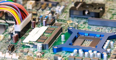
PCB design follows a specific workflow involving schematic capture, PCB layout, and generation of outputs. Where should thermal analysis and reliability enter in to the standard PCB design workflow? These considerations arise at multiple points during design as thermal management challenges create reliability problems in components and the completed PCBA.
Thermal management in your printed circuit board focuses on directing heat from hot to cool areas, ultimately reducing the temperature and producing an even temperature distribution throughout the printed circuit board. Your arrangement of components, the PCB stackup, and other components can be used to direct heat away from an assembly and into the enclosure, or it can be carried away with forced airflow. Design software that integrates with an external field solver will help you qualify your PCB stackup and eliminate hot spots in the PCBA during operation.
PCB thermal analysis can involve multiple tasks that are intended to evaluate heat transfer through the structure of the PCB. This requires pinpointing where heat will be generated and the expected temperature of components during operation, as well as understanding how the structure of a PCB substrate will aid heat transport. Unfortunately, these are complex multiphysics problems that involve field solvers to fully evaluate. Once airflow is driven through the PCBA, the effect of airflow before prototyping can only be evaluated with CFD simulations, something with which not all designers may be familiar.
Designers that have access to these advanced field solvers should use PCB design software that can interface with PCB thermal analysis software within the standard workflow. Before exporting into a PCB thermal analysis tool, there are some simple steps a designer can take to help manage heat generation in the board and prevent excessive temperature rise during operation.
Identify High Temperatures and Prevent Hot Components
PCB thermal management focuses on three principle areas:
- Identifying excessive temperature rise in components and in the board substrate
- Selecting board materials to provide heat transport and produce an even temperature distribution
- Moving heat from hot to cool areas via airflow or conduction
PCB thermal analysis software can help with these tasks at various points in the design phase. The best time to use PCB thermal analysis software is once the PCB layout is completed but before prototyping. However, if you can implement some basic analysis strategies before exporting your design into a PCB thermal analysis software program, you can reduce the extent of any required redesigns with some best practices for thermal integrity.
Component Heating
One step you can take to aid thermal analysis and ensure you’ve identified any hot components in the board is to use thermal resistance values for components to determine their operating temperature. Some components will obviously run at very high temperatures, such as large processors with high I/O counts. However, other smaller components may get very hot even though they can run within their operational limits. LDOs, PMICs, MMICs, and some ASICs are great examples. Identifying these early may help inform where to place these on the PCB so that they receive airflow or connect to a heat sinking element or back to the enclosure. Another possibility is to separate these parts into different areas if possible so that large hotspots do not develop in one area of the board.

DC Power Loss
DC power loss is one contributor to heat generation in a PCB, particularly in power electronics. Smaller digital design and most analog designs will not need this type of simulation. However, power electronics need to ensure power is transferred with minimal loss as this will help minimize heating and maximize power delivery efficiency. DC power losses in your system can be evaluated with a PDN analysis simulation, which will calculate DC power distribution in the PDN.
While a PDN analyzer does not directly show you the amount of heat dissipated or the temperature in your PCB layout, it will show you where hot spots in the PDN are likely to occur. Simple changes can then be made to help improve the integrity of the design and prevent board-level failures.

PCB Material Selection and Stackup Design
Material selection in a PCB requires choosing a resin and curing agent system, material thickness, and copper weight. The thickness of dielectric layers between hot copper regions and nearby planes is also important as it determines how easily heat can be transported around the PCB.
- Copper weight: Boards with heavier copper weight can withstand higher current for a given target equilibrium temperature.
- Resin content: Prepregs with higher resin content will tend to have higher thermal conductivity. These materials may also be preferable in some power electronics, such as in high voltage boards.
- Glass transition temperature: Any board that will experience large thermal excursions should have a high glass transition temperature. Typical high-Tg laminates will experience a glass transition at 170-180 °C.
- Plane layers and laminate thickness: Placing a plane layer closer to a hot area of copper will help remove heat from the hotter region and transport that heat to other areas of the board.
After selecting these specifications on laminate materials, you can build the PCB stackup and send it to your fabrication house for validation. Make sure you understand all the relevant material properties of PCB laminates when selecting materials.

Once these design tasks are completed and the PCB layout is finished, the design can be exported into an intermediate file format for use in simulations. An external tool should be used for comprehensive thermal simulation and analysis before finalizing the PCB and preparing for production.
What to Watch For in PCB Thermal Analysis Software
Inside your PCB thermal analysis software, your goal is to determine the equilibrium temperature distribution given typical operating conditions for the PCB assembly. The simulation results you generate for your PCB should show the temperature distribution in space, as well as additional information on deformation if possible. However, if the equilibrium temperature is known in different regions of the board, it’s possible to estimate deformation from these data.
3rd party field solver applications like Ansys that interface with Altium can be used to run these simulations. These powerful tools can be used to determine deformation in the PCB due to thermal excursions, thermal shocks, and thermal cycling. The combination of these tools gives you everything you need to assess reliability in your PCBA as fatigue failure is an important point to examine in a PCB layout.
Learn more about PCB thermal reliability evaluation.

When devices are running at higher temperatures and significant heat reduction is needed, airflow is often added to a design alongside heat sinks, thermal compounds, and additional copper. The effectiveness of fans that provide airflow, or natural convection, can be evaluated using CFD-thermal co-simulations. These more advanced field solvers help you examine how heat spreads around the PCB due purely to airflow. Additional points to consider in the PCB layout include the mechanical placement of the fan, which requires an MCAD tool to prevent interferences and design the enclosure for maximum heat dissipation and airflow.

Share Your Thermal Simulation Models With Altium
Altium is already the industry-standard PCB design software package, providing the highest quality set of design and manufacturing tools needed to create advanced electronics. Users can expand their design and simulation capabilities using an external PCB thermal analysis software package that interfaces with Altium via an intermediate file format.
The current tool in Altium for generating these simulation model files is the EDB Exporter extension, which will create an EDB file from your PCB layout for use in Ansys field solvers. Altium makes it easy to share these simulation model files with a collaborator, hold them in a project and place files in version control, and release all project data to manufacturing.
Interface With External Field Solvers Via Altium
Altium gives users a unique way to interface with external field solver applications for PCB thermal analysis. Altium users have multiple exporter utilities available to generate vendor-specific and vendor-neutral files for use in PCB thermal analysis software. When you generate these files, you can easily share them with your design team and collaborators. Sharing is secure via a cloud platform and includes a built-in Git-based version control system.
- Altium gives users everything they need to create advanced electronics and prepare circuit board layout documentation.
Learn more about Altium’s complete toolset for printed circuit board design. - Altium includes many extensions to expand the capabilities of the design environment, including an EDB file exporter to interface with Ansys thermal simulation applications.
Learn more about the Ansys EDB Exporter extension for Altium. - Altium is ideal for storing and sharing all your project data, including simulation models for use in advanced field solver applications.
Learn more about using Altium to share your simulation models and data.

Altium delivers an unprecedented amount of integration to the electronics industry until now relegated to the world of software development, allowing designers to work from home and reach unprecedented levels of efficiency. Once you’ve shared your thermal simulation model with collaborators, they can place comments in the design and suggest modifications to help ensure the highest level of quality and reliability. Once a design is finished and is ready for release to production, Altium lets you release your designs into production via an online platform or through the standard toolset.

About Author
Related Resources
Related Technical Documentation
Table of Contents
Design to Release, Without the Friction
- Keep reviews tied to the right version
- Reduce handoff confusion and rework
- Spot sourcing and release risk earlier
- Work solo, share when needed
Get Started
Thank you, you are now subscribed to updates.

