


Pi.MX8 Project - Board Layout Part 4


Chapters
1
2
3
4
5
6
Board Layout Part 4
| Created: July 23, 20247
PCB Assembly
| Coming SoonWelcome to a new installment on the Pi.MX8 compute module SoM project! In this update we will be putting the finishing touches to our PCB design and getting the design ready for prototype production.

In the last article we completed the routing of the signal layers. This was the most time-consuming part of the PCB layout for the Pi.MX8 module. However, we still have two tasks ahead of us that require just as much care: routing the power planes and signal delay tuning.
Power Planes
Let's start with the power planes. I usually like to do the delay tuning as the last steps, as the meanders needed for length tuning often fill up the remaining space on the board. For example, placing additional VIAs (which can sometimes be necessary when routing power nets) might require us to adjust length tuning primitives to create the necessary space. By filling the remaining space with length tuning primitives last, we can avoid additional rework.

Available power plane layers
Looking at the layerstack we can see that we have two dedicated power plane layers available. These layers are separated from the adjacent ground layers by a thin prepreg. This stacking increases the low inductance plane capacitance and can help to decrease the PDN impedance at high frequencies.
Let’s first route the high current power rails. In our case, these are the core and memory rails for the i.MX8 SoC and the DRAM controller with the LPDDR4 IC.

PMIC core and memory supply for the SoC
The VCC_ARM and VCC_SOC rails use remote sensing, which means that the feedback node of the buck converters is not routed to the output capacitors near the MIC, but to the power pads of the i.MX8. This is to compensate for the voltage drop across the power plane or polygon. As the current in these rails can be relatively high and the PMIC needs to regulate these voltages precisely, it is important to "measure" the voltage directly at the load. The following figure shows the voltage drop across a power polygon:

Voltage drop across power polygon
The power polygon for the VCC_ARM rail is routed on layer 6. The trace routed close to the outline of the polygon is the remote sensing signal. Ideally we would like to measure the voltage differentially to compensate for the parasitic effects introduced by the return path current and to make the feedback less susceptible to noise, but in our case this won't be necessary. We will follow the recommendations of the reference design.

VCC_SOC polygon
The feedback trace uses a 'net-tie' close to the pins of the SoC to connect the feedback net to the power net. Without using a net-tie, we'd have to manually ensure clean isolation between the feedback trace and the power polygon. This approach is prone to error. The net-tie is simply a footprint consisting of a short trace segment with two small pads at either end. By setting the component type to net-tie, Altium Designer won't create a short-circuit error for this component.
The VCC_ARM polygon and the DRAM power rail are routed in a similar fashion on Layer 5.

VCC_ARM highlighted and DRAM power rail in purple
The remaining power rails are distributed on layers 5 and 6. The 1.8V and 3.3V system power polygons span the entire board as many components connected to these rails are distributed across the board.
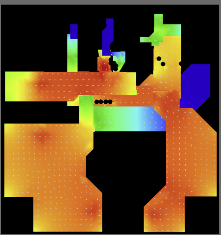
The final step of the power plane routing is to set up an AC and DC PDN analysis and check if the results are within the impedance value boundaries set by the hardware design guide of the SoC.
The AC simulation must include the decoupling capacitors with an accurate equivalent model, the buck regulator output characteristics and the geometry of the layout. We won’t go over the simulation setup in this article but need to keep it in mind as a mandatory verification step.

Power rails target impedance
The DC simulation requires only the layout geometry and SoC load characteristics as input to calculate the voltage drop across the power polygons and highlight areas of excessive current density.
Delay tuning
With the power network layout completed, we can now move on to the last item on our to-do list - delay tuning.
There are many interfaces on the Pi.MX8 module that have strict timing requirements and require delay tuning. We’ll look at the most critical interfaces and see how we can use X-Signals to tune delays even across several components.
Let’s start with the DRAM interface. The i.MX8 hardware design guide provides all the information we need for the delay tuning. Before we can go ahead adjusting any traces we first have to check if the package delay is included in the schematic library symbol.
NXP provides package delay times, which is the time it takes a signal to travel from the i.MX8 BGA ball to the silicon chip. The different lengths on the interposer affect the total delay time, so it is important to take them into account.

Pin package delay in the schematic symbol
We can use the schematic lib list editor to paste all the pin package delays from the i.MX8 hardware design guide document at once using the smart grid paste dialog.

Pin delays in table format through the SCHLIB List toolbar
The delay tuning requirements for the LPDDR4 interface are outlined in the i.MX8 hardware design guide. The guide clusters the delay dependencies into clock, control/command and byte groups. The timing windows for each group are referenced to the clock and strobe signals. All the differential signals must be matched to 1ps between the complementary signals in the pair.

LPDDR4-4000 PCB delay tuning requirements
The signals in the address/command/control group must meet two timing requirements. One requirement defines the maximum delay between each signal within the group, while the second requirement defines the maximum delay window of the whole group referenced to the clock signal.
This is why we use multiple X signal groups to ensure the correct signals are targeted within the design rules.

X-signal classes for the LPDDR4 tuning
When using interleaved delay tuning rules, I like to additionally keep track of the total delay values in an Excel sheet for documentation purposes. This step is optional though and depends on personal preferences as the timing requirements can all be defined within the Altium Designer rule setup.

Delay tuning documentation in Excel
Once the X-signal classes have been defined and the design rules are in place, we can start to tune the delay in the layout. Apart from the intra-pair delay tuning, most adjustments must be made on the address/command/control lines:

Delay tuning address/command/control lines
The data lines themselves need very little to no tuning at all. Around the clock signal pairs routed on the top layer we have plenty of space we can use for delay tuning:

Clock delay tuning top layer
As with the power delivery network we need to perform verification simulations for the DRAM interface. We are particularly interested if we can see crosstalk effects as parts of the routings are packed relatively close together. The rule of thumb is to keep a distance of 3x the dielectric thickness to neighboring traces. We will not be going over the simulation setup and details in this article however.
Once the DRAM interface delay tuning is complete, let's take a look at another application for X-signals. The PiMX8 board has two interfaces that can drive an external display - LVDS and MIPI-DSI.
MIPI-DSI also uses low voltage differential signaling (LVDS), so we can use a multiplexer to select either of these interfaces as they share the same hardware specifications. When using a multiplexer to switch between the interfaces, we also need to be aware that any routing done after the multiplexer (on the common side) will affect the delay of both the downstream MIPI-DSI and LVDS interfaces. This can be taken into account by creating a separate X-signal class for the MIPI-DSI interface and the LVDS interface, allowing more freedom in delay tuning on the PCB.
In this example, it might have been possible to avoid the need for this approach if all the routing on the common side had been tuned to a tight delay window, both inter-pair and pair-to-pair. By using two separate X-signal classes though we have better control over the timing budget of each interface.
X-signals allow us to bridge the gap over the multiplexer and perform length tuning on each interface over the whole signal length before and after the multiplexer.
The same approach is used on the PCIe interface to bridge the gap across the series AC coupling capacitors.

LVDS routed to the multiplexer

MIPI-DSI routed to the multiplexer
All high-speed interfaces on the Pi.MX8 board are delay tuned using X-signals as they provide a more precise path length of the whole signal. We won’t look at every interface separately as the delay tuning rule setup and routing adjustment is a repetitive task that does not differ much in its general approach between the interfaces.
This was the final step in completing the routing on the Pi.MX8 board. The next stage is to perform a thorough design rule check and export the manufacturing dataset.
In the next update we'll take a look at the boards and start assembling some prototypes. This will be the final step to powering up the Pi.MX8 module for the first time, so stay tuned!

About Author
Related Resources
Related Technical Documentation
Design to Release, Without the Friction
- Keep reviews tied to the right version
- Reduce handoff confusion and rework
- Spot sourcing and release risk earlier
- Work solo, share when needed
Get Started
Thank you, you are now subscribed to updates.

