


Pi.MX8 Project - Board Layout Part 3


Chapters
1
2
3
4
5
Board Layout Part 3
| Created: June 24, 20246
7
PCB Assembly
| Coming soonWelcome to a new installment of the Pi.MX8 open-source computer module project! In this series, we delve into the design and testing of a system-on-module based on an i.MX8M plus processor from NXP.
In the previous update, we completed the layout preparations. This included creating the impedance profiles, adding the design rules according to the board manufacturer specifications and defining areas where special design rules should apply. We have also finished routing the LPDDR4 interface but without length tuning (for now).

Before we start with the length tuning of the DRAM interface, we will have a look at the routing of the remaining interfaces on the Pi.MX8 module. There are quite a few high- and low-speed buses on the board, some of which are wide parallel buses that take up a lot of routing space. In order to allocate enough space to each interface, we will first create a rough floor plan for each routing layer on the module.
Routing planning
The routing plan will help us determine how to distribute all of the high- and low-speed interfaces across the available signals layers. By setting up a rough guide in advance, we can ensure we have enough routing real estate available on the layer we are currently working on. This also helps us to minimize layer transitions and reduce the amount of rework to be done during the routing process.
There are several ways to set up layout planning, mainly depending on the tools available. We just need a basic drawing tool that allows us to sketch over an existing image. In this example, we will use Inkscape.
In Inkscape, we can add a background image that shows the component placement and the unrouted interfaces in the form of colored airwires. Note that the power nets are hidden in this screenshot as we will only be focusing on the nets that will be routed on the signal layers. In the schematic, we have placed a net class directive on each power net, making it easy to identify which nets are routed on the plane layers by simply enabling or hiding the associated net class in the layout editor.
For the actual routing, we simply add lines in Inkscape to represent the interfaces we want to route on the corresponding layer. We can adjust the width of these lines to represent how many signals will be routed in the interface. The color of the line can be chosen from the background image to make it easier to identify which interface is being represented.
Since layer transitions also need space allocated on all layers, we can add a block at the end of each line detailing the layer transition.
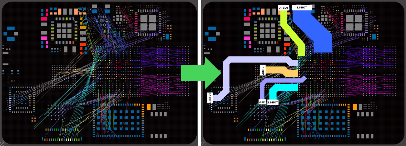
Layout planning in Inkscape with an Altium Designer screenshot as a background image
Once we have repeated the process above for every routing layer we can go ahead and get started with the actual routing process.
Top layer routing
With a routing strategy in place, let's start by routing the interfaces on the top layer. Since we've already done the fanout routing for the components on the top layer, we can use all the remaining space for signal routing. There isn't a lot of space left, but what we have can still be used to make routing on the inner signal layers easier by strategically placing VIAs in regions that won't interfere with routing on the inner layers later. This is another benefit of planning a layout in advance, otherwise these regions would not be defined at this stage.

Top layer routing of the PiMX8 module
When placing traces on the top layer we should also consider that we need some space to add features such as fiducials or labels on the top layer. Laser-etched data matrix codes may also require either a solid copper area or an area with no traces to provide homogeneous contrast, meaning that these areas cannot be used for routing.
Inner Signal Layer routing
Most of the connections will be placed on the two inner signal layers that we´ve defined in the layer stack manager. Let's start by routing all the high-speed synchronous interfaces. In our case, these could be the MIPI-CSI, MIPI-DSI and LVDS interfaces. These interfaces all use low voltage differential signaling and carry a dedicated clock line and at least two data lines. They require a lot of routing space because the length of each data line must be matched to the clock line within a certain timing margin. Matching the length of multiple differential pairs can require a lot of space, as it is very likely that one or more pairs within the interface will introduce a significant delay that must be accounted for. By routing these interfaces first, we can make sure that enough room will be available for the length tuning later.
Placing return path VIAs close to the layer transitions of these high-speed differential pairs is also important to ensure signal integrity. The return path VIAs can take up space on multiple layers, so these VIAs should be placed as soon as a signal transition is placed.
Next, we can route the other high-speed interfaces such as PCIe, USB, HDMI and Ethernet. These interfaces have less stringent requirements for length matching between pairs, so we don't need to devote as much space to length matching. A solid return path management and basic high-speed design approaches on these signals is still very important though placing them second on the routing priority list.
Last but not least, we can route the remaining lower speed interfaces such as SDIO, GPIO, RGMII and other miscellaneous buses such as UART or I2C and SPI. These interfaces still operate at high edge rates, which means we still need to treat them as high-speed signals.

Routing inner signal layer 1

Routing inner signal layer 2
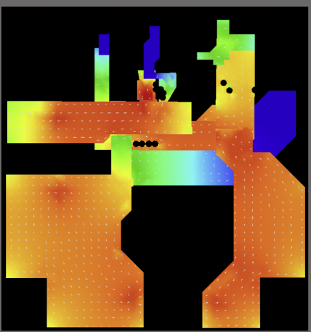
Bottom Layer routing
In the case of the PiMX8 board, we can treat the bottom layer as an inner routing layer in terms of available space. Most of the active components are placed on the top layer of the module, leaving only a handful of voltage regulators and passive components such as decoupling capacitors and configuration resistors on the bottom layer.
The routing priority on the bottom layer is the same as for the inner layers, so we will start with the MIPI-CSI, MIPI-DSI and LVDS interfaces. On the PiMX8 module, a high-speed multiplexer can select between the DSI and LVDS ports. This component is placed on the bottom layer close to the board-to-board connector. Due to the pinout of the multiplexer, there is a significant delay on one of the signal lines connected to the mux. We will have to look at this more closely during the length matching process, but we need to reserve some space on the bottom layer to allow for a larger delay.

Multiplexer pinout with one long line in the interface

Bottom layer routing PiMX8 module
There are a few scenarios on the PiMX8 module that require special attention during delay tuning. We will make extensive use of X-signals to overcome some of these challenges. What exactly these challenges are, and how we can implement X-signals to provide precise delay tuning over a component shared by multiple interfaces, will be part of the next update. Stay tuned!

About Author
Related Resources
Related Technical Documentation
Design to Release, Without the Friction
- Keep reviews tied to the right version
- Reduce handoff confusion and rework
- Spot sourcing and release risk earlier
- Work solo, share when needed
Get Started
Thank you, you are now subscribed to updates.

