


Power Integrity and Simulations with Heidi Barnes

At a Glance
What a very insightful discussion with Heidi Barnes of Keysight. In this episode, we will discuss all things simulations and power integrity in detail. We will dive into EM simulations, capacitor placement, Z, Y, and S parameters correlation measurements, and more!


What a very insightful discussion with Heidi Barnes of Keysight. In this episode, we will discuss all things simulations and power integrity in detail. We will dive into EM simulations, capacitor placement, Z, Y, and S parameters correlation measurements, and more! You will learn a lot from this episode!
Listen to the Podcast:
Download this episode (right click and save)
Watch the video:
Show Highlights:
- Heidi’s background and her 30 years of experience in the PCB design Industry
- When she was only 17, she did an internship at Bill and Dave in Santa Rosa, which is now the Hewlett Packard (HP)
- She got into the solar industry and aerospace
- She is currently passionate about signal integrity and power integrity
- Heidi stresses the importance of simulation tools and mentions the need for having reasonable rules of thumb and have an understanding of what to expect before you jump into a simulation tool
- The Keysight’s PathWave ADS ( Advanced Design System) environment, what does it offer?
- Running an EM simulation and getting results through the pro environments– PiPro (power integrity pro), SiPro (signal integrity pro)
- On top of the DC analysis, it features a lot of great asymmetric tolerances analysis, current density, and thermal heat up effects analyses
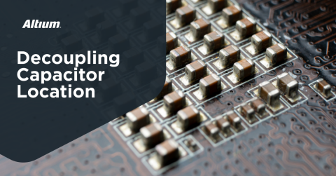
- Heidi talks about capacitor placement–lowering the path inductance, allowing a higher frequency, and giving a broader power delivery from the printed circuit board.
- Capacitor Placement paper presented at DesignCon
- Addressing specific peaks that are exceeding the target impedance in a problematic PCB
- Heidi’s take on using ferrites
- Steve Sandler has a great video about How to Design for Power Integrity–how to select a regulator
- Z, Y, and S parameters–understanding simulation to measurement correlation
- Heidi wrote a paper on SI Journal website: Power Integrity Fundamentals: Impedance vs. Frequency
- She also tackles the “two-port shunt impedance measurement”
- Watch for another episode with Heidi Barnes, tackling subjects related to all things SI and especially getting into measurement issues, coming soon!
Links and Resources:
Check out Heidi Barne’s articles on SI Journal website
Visit Keysight website
Read a previous interview with Heidi Barnes: Heidi Barnes, Senior Application Engineer and Power Integrity Product Owner
Watch Heidi Barnes Altium 2022 Presentation: What is Target Z and Why is Power Delivery AC Not DC? - AltiumLive 2022
Connect with Zack on LinkedIn
Full OnTrack Podcast Library
Altium Website
Download your Altium Designer Free Trial
Learn More about Altium enterprise solutions
Altium 365: Where the World Designs Electronics
Claim the special offer for Podcast listeners only
Zach Peterson:
Whatever AC fluctuations might be either on the rail, ferrite bead is great for that.
Heidi Barnes:
Right. And there may be, like I said, Eric Bogatin is famous for his quote. It depends and so-
Zach Peterson:
I can't tell you how many times I see.
Heidi Barnes:
So we're hesitant to say, never use beads, but people use them incorrectly so often that you get people like Lee Richie and Steve Sandler, just throwing up their hands and saying, never use them.
Zach Peterson:
Hello everyone. And welcome to the Altium OnTrack Podcast. I am Zach Peterson, your host. And today we are talking with Heidi Barnes. Heidi is the product owner for Keysight PathWave Power, integrity tools. We're going to be talking all things simulation, SI and PI, and hopefully some EMI EMC. And I think it should be a very fun discussion. Heidi, thank you so much for taking the time to join us today.
Heidi Barnes:
It's a pleasure to be here and have the opportunity to talk about my latest passion, which is power, integrity, and simulations. And of course always, I do enjoy simulation to measurement correlation. So we'll cover a lot of topics today.
Zach Peterson:
You're speaking my language when I was doing a lot of research in optics, I had to do everything. So simulation plus the measurement correlation, lots of fun. So definitely important. I think for engineers to know how to do that, especially in electronics with test and measurement being so important.
Heidi Barnes:
Yes. And I'm sure that we are both a little bit dangerous with that soldering iron.
Zach Peterson:
Yeah. Sometimes a little too dangerous, right? So Heidi, I'm very interested to first know maybe a little bit about your background. I think some folks in the audience may not be familiar with who you are or what your experience is. So maybe if you could introduce yourself, I think that would be really helpful.
Heidi Barnes:
So I don't know how far you want to go back. I have actually been in the industry for quite some time and very excited to say that I got my start with Bill and Dave, the original Hewlett Packard in Santa Rosa. I was able to get an internship when I was only 17 years old in high school. And I did learn my soldering on the assembly line at HP. So that's where I got my start and got that they had the opportunity to also do some projects with real engineers, that were designing the instruments, the network analyzers and spectrum analyzers back then, however, I have to admit, they got me very excited in their fab area. I got to do a project, actually building some solar cells on the side. And that sort of led me off into a different direction for a while.
I got into a solar cell industry, then I did aerospace and finally came back to Hewlett Packard. It's a wonderful company, wonderful people, and have had the opportunity to work in RF Microwave Packaging, and then be involved with simulation software. So like I said, I've been in the industry for nearly 30 years now. And my latest passion is signal integrity and power integrity. And I've recently done a lot of publications and we're getting ready for even more at DesignCon 2022 in April. And I'm working with Jack Carrell of Xilinx and Steven Sandler of Picotest on some more power, integrity papers.
Zach Peterson:
Yeah. Steve Sandler, someone who I hope to have on. And I actually want to ask you something about an application note that you guys are mentioned in together, coming up when we maybe start talking about simulation and then correlation to measurement. But I mean, it sounds like from your background, because I'm always interested to hear people's backgrounds, especially in folks who are more experienced than myself. It sounds like from your background, you didn't necessarily start with simulation. It sounded like, like you said, you were working on the assembly line and then later on, after coming back to HP, getting into simulation, what drove that shift for you, were you always like a math person that was interested in this kind of stuff?
Heidi Barnes:
Well, I have to admit, I did go to Caltech, which is a notorious for science education and an excellent school. I have to thank the Caltech education for a very broad, well grounded, highly mathematical background in mechanical electrical physics, it was a really good background that allows me to bounce around between applications and technology. The thing I think that everyone realizes at some point is you really want to, and that's probably the Caltech background, the physicist in me, you really want to predict what's going to happen. And you really do need simulation tools. The complexity of the things that we're building with the technology that today is just fascinating. And you don't get there without simulation tools.
Zach Peterson:
Yeah. I totally agree my approach to simulation if you probably haven't read any of my papers or anything, but it's kind of been a mixed numerical and then analytical approach. But I agree with you eventually, at some point you need some of those capabilities that something like probably some of the Keysight tools and then some other field solvers can provide, simply because as you said, the boards get so complex that analytical formulas start to break down and you really have no choice. You have to take some kind of numerical approach to power, integrity, signal, integrity, EMI those types of things.
Heidi Barnes:
Correct. But we also have to give credit to, I think someone like Eric Bogatin, who really emphasizes the necessity to have good rules of thumb and have an understanding of what to expect before you jump into a simulation tool. And so I think that's where, being grounded in simulation and measurement makes us honest.
Zach Peterson:
I totally agree with you. And actually when we had them on the podcast, I had made the point that sometimes if you're using a calculator application or a simulator application and you move the variables the wrong way, you get something that you don't expect, or you didn't know what to expect. I think sometimes people start thinking, well, is everything that I know incorrect suddenly, and then you start questioning yourself. So I totally agree with you having that knowledge of what to expect kind of in the "ideal situation" is actually really helpful, especially when you start going to correlate things to measurements and then maybe making modifications to a layout and then to see how things change. So, you work in power integrity, like you said, specifically, PI simulation tools. I mean, what does Keysight offer for whether it's the all team user or some other user group within the PCB design industry to really help expedite PI analysis and then identify those problems and possibly make changes to the board along the way to getting to the perfect layout?
Heidi Barnes:
One of the reasons that I have to admit, I particularly enjoy the PathWave ADS environment. It has been around for a long time, had its beginnings in the, I think eighties with MDS. And then we moved into the nineties with the ADS, we call it advanced design system. And it's a really unique environment that brings together your layout, your schematics, your data display analysis. And I look at it as an engineering tool and it's not necessarily, one of your enterprise PCB fabrication tools. It's targeted towards the engineer. And we were just talking about how you need to get some simple rules of thumb, know what to expect. And then you want to dig deeper and really apply those very advanced, complex simulation tools like EM simulators and the ADS environment.
I think it's really an engineers, what an engineer needs in the sense that you can start with very simple schematic simulations. You can import your complex board very quickly into layout. You can then go into an EM simulation environment. And one of the things we've been doing more recently is realizing that EM simulations is, finite element analysis, method of moments, finite time, difference, FDTD type simulations. All of these EM simulators can be rather complex if you're not an EM guru and spend your life, setting up these simulations. So more recently we've done, we call them the pro environments and we have PIPro for power integrity, signal, integrity, SI pro. And they really say, Hey, we know you're simulating a printed circuit board. We know some of the analyses that you need to do. We're going to take care of the hard part.
And so these net based, EM tools bring in the printed circuit board, you select components. We know what pins they have. We can say, Hey, you want to simulate this power net? Well, you select the VRM source and the sink we know which pins have the power nets on them. We know which pins have the ground nets. We can place ports. We can get things set up very quickly and get a power integrity engineer up in a matter of minutes, running an EM simulation and getting results. And along those same lines, we start to look at the workflow and we talked about, know what to expect, make sure you have a good solid starting point. And I can't say it enough. And even Steve Sandler says, you're right. You got to start. You have to start with a DCIR drop, make sure that, your board in ports correctly, that your simulation is making sense, that you're actually getting the voltage from your regulator to your sink in power integrity.
And then you start building the complexity. And so on top of the DC analysis, we've got a lot of great asymmetric tolerances analysis, a lot of current density things you can look at just, and then thermal, we can look at thermal heat up effects. Then it's really easy to copy that setup to an AC analysis and start sweeping the frequency to see what your board will do at higher frequency. And this brings up a great topic. We always think of power delivery as DC. We need some DC power, but there is no load out there. That's, how do I say, there is no digital load that is DC power delivery is AC. And the challenge that designers have nowadays is the regulator is really delivering low frequency power. There's a whole range of mid-range frequencies, where your printed circuit board with its decoupling capacitors is the power source to the load.
And that's really the challenge that most engineers have is how do I make sure that transition from the VRM to my decoupling capacitors, and then to the on-dye package capacitance and dye capacitance, how does that delivery of power make that transition to my onboard decoupling capacitors? And then as I go up in frequency, transition to the package dye, and that bring us to the RF microwave world of matched impedance. But again, so that's, that AC power delivery, the optimization of the decaps, that's sort of that methodology that you need to look at there. And then most recently, one of the things that I think is a pain point or people are struggling with, as we start to manufacture or want to say, looking at designing products is that EMI EMC problems are very challenging because it's hard. It's a little bit harder to understand what's generating that EMI EMC noise.
And there's some very strict guidelines now that are coming out, especially for automotive with the 25 standard. And you really don't want to wait until your product is finished to find out that you're failing and then try to band aid things and try to do modification or even, if you have to respin the board, you are obviously delaying your launch and everything. So, and again, EMI EMC simulations are one of the more complex simulations to do, because they're differential excitation and that common node current is coming back on a return plate or a different path. And getting that simulation to work is a challenge, but is something that we are trying to make available to your common power, integrity and signal integrity engineer.
Zach Peterson:
Sure. And I think you brought up an interesting point, which is, how the board effectively is your power source. Once it essentially charges its capacitance charges up, I was actually talking with someone who left a comment on one of our YouTube videos and it was along the same vein of when do you choose more capacitors versus when do you choose maybe another power and ground plane pair to bump up the board playing capacitance. And my view was looking in the frequency domain. You can actually, if you like try and target specific regions of the impedance spectrum with certain capacitors, if you're crafty enough, I think some people have to learn a little bit of pull zero analysis to be able to do that. But then when do you actually say, you know what, I have enough capacitors and then I'm going to instead opt for the plane pair to then bring down the overall impedance at these higher frequency ranges, does Keysight kind of help make those recommendations?
Because we talk sometimes about capacitor optimization, like when do you have enough capacitors and when is the solution now just okay, instead of taking my bank of 50 capacitors and doubling it, do I instead just go for a power ground plane pair?
Heidi Barnes:
Right. And I have to be honest, I am not very adept with polls and zeros and the traditional sort of analysis. I have been working very closely with Steve Sandler and I come from an RF microwave background and I've watched a DesignCon the signal integrity world just, make an about face. And they use S parameters everywhere and they understand impedance everywhere now, you don't have clamping diodes to prevent overshoot. You now match impedance and things like that. So power integrity is similar. It's amazing what you can do if you trans go from the time domain to the frequency domain and start doing your design and the frequency domain. And that's where target impedance comes from a long time ago, started doing papers at DesignCon about, target impedance, look in the frequency domain.
If we can keep the impedance low across a broad range of frequencies, then any dynamic DIDT at a range of frequencies times that low impedance will result in a low Delta ripple or voltage ripple. What I have found and what Steve Sandler is brilliant on is if you start, it's very easy in simulation, I can start it by taking all the capacitors off and I can have a model for the VRM. I can have a model EM model for my printed circuit board, and I can have a model for the package dye, and I've done this. I did this in past presentations at EMI EMC. I just did a webcast in January on capacitor placement. And what you find, if you take all those capacitors off and you start, there's a big inductance. The impedance starts increasing like an inductor.
Well, if you measure that inductance, it tells you how much capacitance you need. It's very simple. The inductance divided by the target impedance square is going to equal your capacitance. And this kind of goes from transmission line theory. You know that the characteristic impedance Z knot equals the square root of L over C. Well, if you replace that characteristic impedance with the impedance you want for your power plane, then you can solve for the capacitance if you know the inductance. And so it's kind of a really neat little trick there. If you know you have a certain inductance that's increasing with frequency, I am going to pick a capacitor that has the opposite slope. So my inductors going up with one slope, my capacitor's decreasing with impedance with another slope and if I pick that capacitor correctly, it flattens it out. And now you have the capacitor is balancing the inductor it's impedance matched so that your current and voltage are in phase.
It's going to look like a resistor. And I guess I kind of like to say, you've quit. You're not making a swing where you're slosh, you're oscillating, you're actually flowing very, it's critically damped, you're back and forth between that inductance and capacitance without ringing. And so that's your impedance of your power rail and you place... What you find in practicality is that first capacitor that I need is going to be a lot, the bulk capacitors are going to be pretty big. They have a lot of inductance. And so that capacitor that I picked to match the inductance is now only going to make it to a certain frequency. And then the inductance of the capacitor starts to go up. Well, I can look at that inductance with that bulk capacitor. And then I can say that inductance divided by the target impedance square is going to give me the next smaller capacitors that I need to add.
And I just keep matching along, getting smaller and smaller capacitors with lower and lower inductance. And remember, I'm looking at it as I find the sink. So I'm the sink that needs power. And I'm looking back towards the VRM. So I'm including all of the inductance of the path. So the bulk capacitor that is keeping the stability of the VRM, there's a lot of path inductance there, but as I start using smaller and smaller capacitors, I can move closer to the sink and lower that inductance and go to higher frequencies. Now you brought up an interesting point, do I get a thinner power and ground layer to get more capacitance in there? And I always kind of thought, oh yeah, I'm adding capacitance. And I am adding a little bit of tiny, high frequency capacitance, but what's really critical.
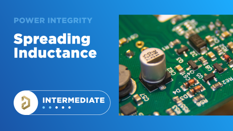
What's more important is the fact I'm lowering the inductance, the path inductance. And what that enables me to do is now, they always say the inductance is the loop. So if I have a capacitor way up high and the ground plane way down below, I'll see this loop between the, I'm sorry, the power plane and the ground plane, there'll be a big loop. If I squish them together, the area of that loop gets much smaller and that lowers the inductance. And then that lets me place capacitors further from the sink, but still have low inductance. So if I can put a very thin power and ground layer, I lower the inductance. It gives me more flexibility as to where to place capacitors. And even underneath the BGA where I have my, say my BGA sink. Even if I am going all the way to the back of the board, my load, my sink is on the top of the board.
My capacitors are on the bottom and I have these vias that have to go up connect between the two, my power and ground vias. What's interesting is even with the power and ground layers, very close together, I've made a very small loop there. So as the power and ground layers get further apart that even that loop within the vias gets bigger.
Zach Peterson:
Yeah, that's spreading inductors.
Heidi Barnes:
Yeah. So anyway, I guess what I was excited to find from my capacitor placement paper that we did at DesignCon, and then I did the webcast in January was this idea that, Hey, the real thin power and ground layer separation is not so much for the capacitance. It's much more for lowering the inductance and then that lets you go to a higher frequency and give a broader power delivery from the printed circuit board. And I'm probably talking a little fast. I apologize. I get excited and it's very fun.
Zach Peterson:
It's fine. It's totally fine. You actually brought up a lot of interesting points here because, you brought up the point, number one, about bringing down the slope, right. By essentially counteracting that impedance, which makes perfect sense. Right. I think pretty much everybody in the PI community agrees and you can see in simple simulations, even if you just do it in SPICE, we actually did a video on this, that adding in inductance is generally bad. Okay. But what if you already have a, let's say you already have a PDN design, you already have a board. It has problems, maybe you've done a spin. You see that it's got too much noise and then you do some simulation of the PDN and then you see these peaks.
So now instead of targeting a slope, you're actually pinpointing specific peaks that are exceeding maybe your target impedance or that you can correlate to a specific portion of the time domain measurement, is now the solution. Do we just triple our number of caps, that's obviously, throwing a hammer at the wall and trying to nail up a picture, but that's the extreme case. Do we just target specific peaks with specific capacitors based on their SRF? Or do we opt for planes?
Heidi Barnes:
So I don't think the planes are going to be a challenge because you have to respin the board, but again, simulators make it so easy. You can go into that simulation environment and you can actually, like I just said, in simulation. It doesn't cost anything. I don't have to get the soldering iron out. And let me tell you removing small caps and putting them back on, they call it tombstoning. They like to pop up and move around with that surface tension on the solder. But anyways, that said simulation makes it easy. And I really try to convince people, look in the impedance domain, do some simple simulations or, it's not that hard to get your print circuit board into an EM tool and realize that if you have a peak impedance and you pick that frequency as the self, frequency of the capacitor, you're not really matching impedance.
You're just trying to put a really low impedance at that peak. And you generally create two more peaks that are HighQ. What you're trying to do is like I said, match the inductance with a capacitance to get the voltage and currents in phase to avoid resonances and be a lot more stable with capacitor tolerances and variations. If you do that classic where you say, I have a peak resonance and I want to make a real low impedance at that frequency, you're now doing what I call a multi pole design, which Steve Sandler has shown a number of times. You're a lot more sensitive to capacitor tolerances and specs because those peaks will start moving around. In the simulation tools like PathWave ADS with PIPro, we have a decap optimization tool that'll help you sort out all those little small capacitor values and find out which ones are maybe causing problems or not needed.
You can design for that flat impedance. But like I said, I would basically pull the capacitors off and start adding the groups of them one at a time. And usually what you find is the very small capacitors do not have a lot of ESR and the resonance that HighQ peak the Q and the how sharp it is and how high that impedance peak is, is basically a function of the, how much real resistance you have to the impedance there. And so you need some real resistance. You need that ESR of the capacitor. And a lot of times when people just throw, lots and lots of small capacitors on the board, they don't realize that they're really lowering that ESR value that parallel ESR of all those caps gets very low.
And now your resonances are becoming very HighQ because there's no dampening resistor. Now on the VRM side with the bulk capacitors, you often hear snubber resistors and that's exactly what they're doing. Their bulk capacitor doesn't have the right ESR. And so they actually put a resistor capacitor and then a resistor in series to add that ESR, that real resistance to dampen out the Q of the residence at the higher-
Zach Peterson:
Essentially-
Heidi Barnes:
It's harder to do that with the small caps.
Zach Peterson:
Well, I was going to say, that's essentially the same type of thing you might do if you're actually designing a VRM circuit. And then you have excessive overshoot during those switching events. And or maybe there's a parasitic or there's too much inductance on your cap. Basically a very small resistor is probably just enough to bring it into the critical damping regime and then actually get smooth power output.
Heidi Barnes:
Right. And if you look in the impedance domain, it's very obvious what's going on there. If you try to, if you're looking in the time domain with a oscilloscope and you see all this ringing, you're like, where is this coming from? And yet, if you look in the impedance domain, you can say, oh, this ringing is, this bulk capacitor or this decoupling capacitor over here, it's much easier in simulation to start learning where those residences are coming from.
Zach Peterson:
Yeah. I agree with you, especially if you're looking in the time domain, because, let's say with an arbitrary time domain measurement, there could be 10 polls that are all essentially being excited all at once by a broadband pulse. And so you get a very complicated time domain readout on a oscilloscope let's say, or in a simulation and all of a sudden it's like, well, how do I correlate this to one specific cap? And I think at that point, it's kind of impossible. And like you say, you have to work in the impedance domain, but maybe you've only got two peaks, let's say, you've got a high frequency peak, and a low frequency peak, and they're superimposed on each other. Then it's very easy to really see, okay, I know I have excess impedance at high frequencies. Now I need to maybe experiment with adding more capacitors or maybe I just know that, Hey, this correlates with the frequency of my plane pair. Now I need to add in another plane pair.
Heidi Barnes:
Right. And so, again, I think the lesson there, I mean, key thing that I want to encourage people to do is not just look in one domain, the time domain and the frequency domain together will give you the complete story and makes the troubleshooting a lot easier.
Zach Peterson:
Yeah.
Heidi Barnes:
I feel like tools make that really easy to do.
Zach Peterson:
Yeah. I agree. Even in SPICE, I mean, just run a transient and run the AC and see where you can get the two to jive together, I guess you could say.
Heidi Barnes:
Right.
Zach Peterson:
So another thing about critical damping, and I think a lot of the designers are trying to do this with bringing a transient response into critical damping without actually realizing that they're doing this, which is by possibly adding a ferrite into a rail on a PDN. Oh, I love the reaction because that's usually my reaction. So I've seen the ferrite used into two possible ways. One is just as a damping element on a rail that is supporting high speed iOS. The other way is to isolate a high speed rail from maybe a lower speed rail or like a PLL rail, and to essentially try and prevent the noise from the high speed rail from propagating over to a different rail. And so, as an isolating element, tell me your thoughts on that. Maybe I can tell you mine, but I'd like to hear yours.
Heidi Barnes:
So buyer beware.
Zach Peterson:
Yeah. Right.
Heidi Barnes:
I guess maybe my really, really simplistic viewpoint is there was a time when your VRM, your load was within the bandwidth or the control loop of the VRM. So your power supply was slow. Your load was slow. And when I put a ferrite bead in there with this, increasing resistance or this resistance at higher frequencies, this inductance, that was okay. Because my load running fast. And I was trying to get, maybe get rid of some noise, but like we talked about my load, my high speed digital load is a high frequency load. It needs power at those higher frequencies. And so the moment I put an inductor in there, this bead, this ferrite bead, first of all, it does have a resistance at the higher frequencies, but it also kind of will turn into a capacitor.
Eventually it's not a perfect inductor. It also will then resonate and ring with other things in your circuit. And on top of that, I'm trying to deliver high frequency power to this load. And you just added more inductance. You made my life harder. I've got to then add more capacitors to compensate for the inductance you just put in there. So you really have to ask yourself, are you saving money or should you go back and say, Steve Sandler did an excellent on YouTube, a Keysight sponsored how to design for power integrity. And one of the first videos he did actually was the second one, I'm sorry, was on how to select a voltage regulator module, a VRM or regulator
Zach Peterson:
I remember that.
Heidi Barnes:
Converter. Yeah. And he is like, pick a current mode VRM because the power supply rejection ratio is so much better and its output impedance stability is much better.
And there's just some simple things you can do with the selection of the VRM. And we did an ADS, like I said, it's an engineering environment tool, very easy to do some money, Carlos sweeps of tolerances set up those BI types, transient simulations, and look at different regulator topology even use Steve Sandler's state space, average model that simulates very quickly with harmonic balance in a matter of minutes instead of hours with transient simulations. Anyway, the thing that we were trying to say there is you really want to understand how the power delivery's happening. If you design it correctly, you're matching impedance, you're getting rid of those resonances. You have a regulator with high power supply rejection ratio. You shouldn't need to be adding the expense of a bead and then having to add even more capacitors to compensate for that extra inductance for your high speed digital loads.
So that's just my feeling there. It also kind of leads into the EMI EMC in the sense that, and let me start, even with a simpler example, we're talking about noise and energy that's going the wrong places. And in the signal integrity world, I always like the example from a transmitter to receiver. If I have a matched transmission line, I don't have any reflections. All the power goes from the transmitter to the receiver. There's no reflections, it's matched impedance. I don't get radiation. All the energy is going where I want it to go. The same thing has to sort of apply to power delivery. If my source, my VRM can be matched with the load. And I have my decoupling capacitors, all being matched and not resonating then across frequency. So all the way from DC into the tens of megahertz, what you find is the power's getting to the load correctly.
There's no resonances since you're not radiating. And that's really what the goal of a power integrity, power delivery network should be, or was a power integrity engineer should be focused on is how do I minimize the resonances, those sources of EMI EMC, how do I provide for that sort of flat versus frequency power delivery, voltage and current in phase. And then you actually solve a lot of problems all at once.
Zach Peterson:
Yeah, absolutely. So one thing I wanted to ask you about with regards to ferrites is in terms of isolation, because there is an older DesignCon paper that shows that if you use the ferrite just for isolation, rather than as a damping element on say like a high speed IO, which I think we can all agree is generally a bad practice that they do get some improvement in noise propagation to this lower speed rail. Whereas another engineer who has actually been published on the Altium blog says the opposite. You actually get worse output on the isolated rail.
So where do those things line up? Is this just a matter of learning how to choose a ferrite bead, should you choose to try and do this in a power PDN design application where you're isolating two rails, or should you take the Lee Richie approach and say, I've never used a bead. I just engineer the capacitance and I agree with Lee Richie on this, you probably don't need the bead if you can engineer the capacitance properly. But if you do use the bead, you should definitely learn how to select it properly, and then make sure you actually qualify that in simulations and tests before, or you just blindly follow within an application note.
Heidi Barnes:
Right. And I think my long-winded answer before agrees with Lee Richie, don't use the bead, engineer the capacitance is a very good way to phrase it. And with the simulation tools that we have now today, you kind of ask why aren't you doing some simulation and looking at what's really happening in the frequency domain with those residences, I think probably leads a little bit into the simulation to measurement correlation world. If you're going to use a bead, I highly recommend not just trusting the vendor data, actually got out there and measure in it, find out what is it doing at low frequency, and when does that bead become a capacitor and start doing some strange things at high frequency with your power delivery network.
Zach Peterson:
And when you say measure, you mean measure the actual bead itself, measure the impedance of the bead?
Heidi Barnes:
Yeah. Yes. Get it on a network analyzer and actually, low impedance network analyzer that has the range to look at that bead.
Zach Peterson:
Absolutely, totally agree. I think a lot of people will look in like a reference design and, or they'll look at an evaluation product where the schematics are available and they'll see, oh, I see a bead there. I should probably be doing that on all the rest of my designs. And that's not necessarily the case. I mean, maybe it worked fine on that evaluation product, but that doesn't mean that all your other boards need it. Would you agree?
Heidi Barnes:
Right. Well, I have to, there's kind of a disconnect you go to... There's the companies that make your regulators the big IC manufacturers that have been making regulators for years. And you have to realize when you go out and you look at the data sheets for those regulators and even sell your evaluation boards, the load is resistive. They're focus on the bandwidth of delivering power within the regulators' control loop.
Zach Peterson:
That's a great.
Heidi Barnes:
They don't care about the high frequency. They're delivering power to a resistor. And of course, if I put a bead in there, it kills the high frequency, but they completely miss the point that I have a digital load that needs power at high frequencies. So now what do I do, I just killed my ability to deliver power at high frequencies.
And now I've got a sort of a bigger challenge on delivering or designing my decoupling capacitors. And I think that's the one that people miss. You can use the bead but most people completely fail to adapt their power, their decoupling capacitors to work nicely with that bead. And this brings up a point that Steve Sandler's always making that bead the tolerances on it are horrible. And so now you've got this very widely varying component that you've got to try to adapt to your decoupling capacitors to. And so that's something to, like I said, buyer beware and really understand what you're putting into that circuit in terms of impacting your power delivery at higher frequencies.
Zach Peterson:
Yeah, absolutely. And you brought up the crux of the point, right? The evaluation board is pulling power to a DC load or to a resistive load. So it only needs DC power. Anyways, it doesn't need the DC power. So of course do whatever you can to block whatever AC fluctuations might be there on the rail. Ferrite bead is great for that.
Heidi Barnes:
Right. And there may be, , like I said, Eric Bogatin is famous for his quote. It depends. And so-
Zach Peterson:
I can't tell how many times I see.
Heidi Barnes:
So we're hesitant to say, never use bead, but people use them incorrectly so often that you get people like Lee Richie and Steve Sandler just throwing up their hands and saying, never use them.
Zach Peterson:
Yeah.
Heidi Barnes:
Because they see it used incorrectly. So often nowadays.
Zach Peterson:
Yeah. I try not to give people the never, I try to give people the here's the danger, but I agree with you. I think there are some things where you could say you should probably never unless, and just get a little bit closer to saying never use it.
Heidi Barnes:
Yes. It depends. But a little bit stronger than that.
Zach Peterson:
Yeah, exactly. So I'm sure you, and I could talk about this stuff with PDN engineering for another couple hours, if we really wanted to, but there's one thing I had alluded to earlier that I wanted to ask you about before we go, which is S parameters in power integrity. Now, you look at like the paper that you had referenced, I think it's actually your paper in signal integrity journal where you're looking at inductance and the inductance slope and using that as part of the design. That is your paper, right?
Heidi Barnes:
Yes. I did a basics on power integrity for SI journals.
Zach Peterson:
That's right.
Heidi Barnes:
Good memory there.
Zach Peterson:
Yes. So I will link to that in the show notes. So people can go ahead and read that. Yeah, absolutely. But there was one thing that's actually really interesting with using S parameters over Z parameters because when you're doing a simulation and we're talking about impedance, right. The impedance is basically the Z parameters, right. It's just a transfer function that converts current to voltage, or you can invert it and then you have, I forget, I think the Y parameters or, and conductance parameters?
Heidi Barnes:
Z, Y and S parameters.
Zach Peterson:
Yeah, exactly. And so then you're essentially just transforming voltage to current and whatever parameters set you want to use. But then with S parameters, S parameters rely on a reference you're essentially making comparison between the actual impedance of the system you want to investigate with some reference, normally 50 ohms because we use S parameters so much in RF and everything on the RF side with PCBs is at 50 ohms. Obviously you're aware, but with PDN being such low impedance, you're trying to make comparison between very low impedance, one ohm or less ideally in the milli ohm range with what is normally a 50 ohm measurement. So how do you deal with this to get accurate S parameters because S parameters and their relationship to the error that you get in the S parameters, the S one one or S one two values, I believe are non-linear related to the error that you would get.
So if you have very small PDN impedance and you have a slight error in the measurement due to maybe there's noise, maybe there's imperfect reference, whatever it is that actually magnifies the error that you see in the measurement and you get incorrect results. So how do you deal with measurement of PDN impedances at very low impedances?
Heidi Barnes:
Okay. Well, first of all, one of the reasons there's, you're right, Z, Y, and S parameters and the basic thing is you're, what is it your Z parameters are typically measured with, what is it, the short and then your Y parameters. I think the open at the unused port type thing, the S parameters, you have your unused ports with terminated with a known impedance. And basically what it comes down to is doing shorts and opens at high frequency is not a very, what is it? It's a difficult way to do measurements. And so they found very early on, as you start going up in frequency that measuring Z and Y parameters directly was a challenge. And so that's where they came up with S parameters terminating in the characteristic impedance to reduce those reflections and make it a more realistic or practical measurement to do.
And so now we have this and they settled on 50 ohms. That's sort of the environment for signal integrity, instruments out all over out. There are characteristic impedance 50 ohms for doing those S parameter measurements. And this is where I really do like understanding simulation to measurement correlation. This challenge that measurement world has in actually measuring Z, or Y parameters at high frequency, and then they switch to S parameters. It's easier to measure the S parameter with those terminating, with the characteristic impedance, but once you have that S parameter, now you can do the conversion to Z or Y, you can make that mathematical conversion, but you have to always kind of keep in mind that sometimes there's challenges with how many decimal places that you have. And so that's one of those things that even that the challenge we have in measurement also kind of can be a challenge, even in simulation that we have to keep be aware of with, say if we have a huge reflection and we're trying to measure a small difference, we're going to need a low.
We have a reflection that's 0.9, and we want seven decimal places out there to see the small change in impedance that we're looking at. So that's sort of looking at S one one reflection. That's huge when we're measuring the 50 ohms, and we're looking at a half milli ohm or almost micro ohm impedance, we're going to get a huge reflection. And then if I change that impedance slightly, I still have a big reflection. I just need a lot of decimal places to see the small change. So that's the challenge with, I want to measure impedance. So I'm going to use S one one reflection, and I'm using a 50 ohm measuring in instrument to look at 0.1 or micro ohm impedance in the simulation world. I just say, oh, I'm going to change my instrument to be micro ohm.
And then I can look at that reflection, no problem, but I can't do that in the measurement world. So this is where again, the measurement world gets a little bit creative and did a paper on this, oh gosh, probably early 2000s, 2004, 2006, somewhere in there at DesignCon. But anyways, basically it's a two-port shunt impedance method. And it's really clever because you hook up basically port one to port two on a network analyzer. So you have this nice 50 ohms transmission line going from port one to port two, all the signal goes across. But then if I place a connection in the middle of that transmission line, going from the signal transmission line to the ground, if I connect that to my very low impedance power rail or to a very low impedance bead or capacitor, basically I'm providing a very, like a one milli ohm resistor from that signal transmission line to ground in the middle of it.
And now my signal from port one sees that going 50 ohms traveling along the transmission line and it sees 0.1 milli ohm, it has a huge reflection. And then there's a tiny signal that makes it to port two. Okay. So most of the signal goes back to port one, but the small signal that makes it to port two. Now my network analyzer's very sensitive and I can monitor very small changes in that current that gets to port two. And now I can make very small changes in my low impedance network that I can see. So I can go from 10 milli ohms to micro ohms and I can see how that small change to port two happens. My network analyzer's very sensitive. So this is called a two port shunt impedance measurement. I've shunted the transmission line to ground or through my very small impedance that I'm trying to measure my power rail, my capacitor, and then mathematically, you have to look at how do I convert that?
How does that S two one signal that makes it to port two equal impedance? And that's where people struggle because I'm taking an S two one measurement, but mathematically, I can say 25 times S two one divided by one minus S two one magically equals Z of my device under test. So that's the one I think that people have to maybe look at the math and read some papers and really get their head around that you can do this S two one through measurement. And yet it's telling me what the shunt impedance is. Now there... Yeah, go ahead.
Zach Peterson:
So it's not a simple matter of say, taking your simulation with a theoretical milli ohm VNA and then changing the reference to 50 ohms and then just measuring it 50 ohms.
Heidi Barnes:
So in simulation, I can do that same. I can match with measurement. And so I can also do a 50 ohm instrument in simulation. And then it's really nice because in simulation, I have a lot of decimal places. I don't have a noise floor that the instrument has. And so I can compare the traditional S 11 reflection, TDR impedance measurement, S 11 to this S two one measurement. I can set up that same sort of SPICE simulation schematic, where I've got a resistor shunting or my low impedance shunting to ground going between 250 ohm terminations. And so I can make sure that my mathematical conversion is correct. I've more recently had some fun, because simulation makes it easy. There's also a transformation assumption you can go from this sort of Delta network of your measurement of 50 ohms on either side with, how do I say with your network analyzer and then your transmission line.
How do I say actually, I've got it back anyways. You can go from this black box model of your measurement that's Delta network. You can convert to a team network and you find that the impedance of the device under test is actually Z two one. So there's also another method of converting your S parameter S one one S two one, and S two two of this shut impedance measurement to Z parameters. And then the Z two one is the impedance you're looking for. And again, I'm kind of talking fast here and it's definitely something that you want to sit down and kind of work through the math yourself, read some papers on, but it is the method for measuring low impedance. And that is really how you start to correlate your simulations with measurements. If you're designing in the frequency domain with impedances, you better know how to measure it. And the two port shunt method is the classic way of getting those low impedance measurements to correlate with simulations.
Zach Peterson:
So what I'm hearing here now is that instead of just saying, we're just going to do a calculation of maybe the impedance and then just directly compare, you should actually simulate the measurement setup?
Heidi Barnes:
Yes. And people forget to do that sometimes they just assume that the measurement is perfect. And then the, they forget that sometimes when you go and actually put that environment in the simulator, you start to realize some of the, how do I want to say challenges with the measurement and where the sensitivities are in yourself.
Zach Peterson:
Well, then with the sensitivities, because at that low impedance range, when you're comparing, let's say you are comparing to 50 ohms, very slight tolerances can produce a very big change in which you measure. So now you can include the tolerances in the measurement simulation, the simulation of your measurement, let's say, and then you could get a range and say, well, okay, let's say, it's my caps. My caps have 10% tolerance. How does that propagate into a variation in possible measurements that I should see based on those tolerances.
Heidi Barnes:
Right. And again, back to capacitors, you find very quickly, where do I place the reference plane? The capacitor has pads, the plus and minus pad separation, which determines a footprint on the print circuit board. And then I have to connect those plus and minus pads to the power and ground plane. But if I'm measuring... If I measure the capacitor in a fixture, I'm going to get the capacitor plus that mounting inducted. So now, if I have a different board with a different mounting inductance, I want a model of that capacitor without the mounting inductance, because my EM simulator is going to provide that mounting inductance.
I'm bringing a whole print circuit board in I'm actually EM simulating that print circuit board. So I am simulating most of that mounting inductance and trying to optimize it for my topology. You were talking about bringing power and ground planes closer together. So the capacitor model I want is one that doesn't have that mounting inductance. So there, again, the vendors, most of the time have some mounting inductance in there because they assume you're going to put it into a SPICE simulation without a printed circuit board in there.
Zach Peterson:
Oh, okay. So when you say, real quick, when you say mounting inductance, you're referring to the inductance of the vias and then the size of the pads.
Heidi Barnes:
It's a little bit trickier because it's also the distance between the power and ground pads on the capacitor. And so that's where it gets a little tricky. Where do I draw the reference plane? Do I include some of that separation that inductance between the pads, that distance is some of that included in the capacitor model or do I include it in the EM model of the printed circuit board? And Steve Sandler came up with a real simple trick. He said, well, I can measure the capacitor on a board, any stackup I want. And then if I put a measure that board without the capacitor and short the power and ground pads together, it's a very simple measurement. It's very easy to short those pads together. And then I call that loop with the short, my mounting inductance, and I de embed that I can de embed with S parameters it's mathematical de embed of that S parameter of the mounting inductance loop measured with the short, from the measurement of the capacitor, with the mounting inductance.
And then I end up with just what's left over is the capacitor parasitics. And so that's how we've been doing things because I can do a very simple measurement to remove the mounting inductance from the capacitor. And then if I use that capacitor with our PIPro EM simulator, I get the correct combination of just capacitor plus the EM model of the parasitics of the print circuit board mounting inductance.
Zach Peterson:
Makes a lot of sense. Well, we've been going on for a while. And like I said, I think you and I could go for a couple more hours if we really wanted to, but this has been a very illuminating discussion about all things PI and especially getting into measurements. So maybe you and I should schedule another podcast at a later date to maybe talk more about some of these measurement issues, because that's definitely where I came from before getting into PCBs. And it's something that I care a lot about. And I think a lot of engineers should know more about
Heidi Barnes:
Definitely. And I applaud you for doing these podcasts and bringing power, integrity, more attention to the world. And it's exciting to see that you've also worked on these power delivery topics in the past. So wonderful to have the discussion with you.
Zach Peterson:
Well, thank you very much. Thank you. To everybody out there listening today. We've been talking with Heidi Barnes at Keysight. Wonderful to talk to you about these topics with PI and we didn't even touch SI. I'm disappointed. We should-
Heidi Barnes:
I know that's a whole yeah. Another hour.
Zach Peterson:
Yeah. We'll do hour. Number two on SI I suppose. Thank you again. This has been a lot of fun and to all of the listeners out there, be sure to check out the show notes, we'll link to some of Heidi's SI journal papers and you can go learn more about power integrity. To everybody listening, don't stop learning, stay on track and catch us next time for another episode of the OnTrack podcast.

About Author
Related Resources
Related Technical Documentation
Table of Contents
Design to Release, Without the Friction
- Keep reviews tied to the right version
- Reduce handoff confusion and rework
- Spot sourcing and release risk earlier
- Work solo, share when needed
Get Started
Thank you, you are now subscribed to updates.