


PDN Impedance Analysis and Modeling: From Schematic to Layout

At a Glance
Do you know the factors that determine the impedance of your PDN? Here’s what you need to know about PDN impedance analysis and modeling.


Power integrity affects many performance aspects in PCBs, and ensuring power integrity in a digital design starts by ensuring the PCB layout has a low Power Delivery Network (PDN) impedance. There are several basic aspects of PDN impedance and some basic design steps that help a designer reach relatively low PDN impedance in a PCB. Without low impedance, power glitches can cause components in a board to operate incorrectly due to large voltage swings on the power rail, which can then propagate to signals and appear as jitter along the rising or falling edges.
PDN analysis occurs in two regimes: the time domain and the frequency domain. If you can build some reasonably accurate models for PDN impedance, you can then compare transient responses on the PDN with the power fluctuation limits in modern components. PDN analysis also occurs in the frequency domain, which will allow a designer to determine the signal bandwidths and power levels that can be supported in a digital or analog system.
Why Conduct PDN Impedance Analysis?
The goal in designing the power delivery network in a PDN is to ensure DC and/or AC power can get to where it's needed. Power regulators have low-impedance output, thus we would want to create a low-impedance path that can supply power to load components on the PDN whenever power is needed. How power is delivered and dissipated depends on whether we look at AC or DC systems. High-speed digital systems and analog systems will have both components present in some regions of the system, so we need to consider power integrity from both aspects.
DC PDN Analysis
In DC systems with resistive components, power delivery is a relatively simple concept; power is dropped over a load based on the load's resistance. For this reason, DC PDN analysis generally only considers the resistive power loss (IR drop) throughout the conductors leading to loads in the PCB. This requires some calculations of current density in the planes and power rails used for power distribution, which can then be visualized as a color-coded map in the PCB layout.

DC PDN analysis is often ignored as part of digital systems design. However, it is still important as modern digital systems supporting large ICs with many high-speed IOs (such as FPGAs) will need to draw large bursts of current at any moment. To ensure noise-free power delivery, digital systems rely on AC power integrity analysis.
AC PDN Analysis
Delivery of the AC portion of power is more complex and is prone to noise problems. In the past, with TTL components running at high core voltages (5 V saturation logic), it was possible to ignore many power integrity problems because the noise margins on logic circuits in these components were very large. Today's digital components generally run at 3V3 or lower core voltages with thinner noise margins and higher IO count.
In short, the AC PDN impedance will affect the following aspects of your circuits:
-
Power bus noise. Ripple in the PDN voltage is created by transient currents in your PCB that interact with high reactive impedance at certain frequencies. Note that, because your PDN impedance is a function of frequency, the voltage ripple caused by switching will also be a function of frequency. Note that these transients arise regardless of the level of switching noise in the output from your voltage regulator.
-
Damping in power bus noise. The amount of resistance and loss in the dielectric laminate will determine whether the ripple on the power bus appears as ringing (i.e., an underdamped transient oscillation) or whether it is overdamped. This is one problem that can occur if your decoupling capacitor is incorrectly sized or if you do not account for your decoupling capacitor’s self-resonance frequency in your decoupling network.
-
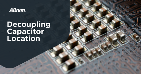
Required level of decoupling. Most capacitors can be insufficient for ensuring decoupling in PCBs with fast logic due to their relatively low self-resonance frequencies (~100 MHz to ~1 GHz). Therefore, designers use small-case/high-Dk capacitors (e.g., 0201 MLCCs) and interplane capacitance to provide sufficient decoupling.
-
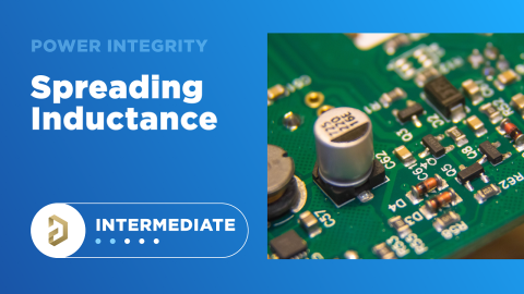
Current return path. Your return current will follow the path of least resistance (for DC current) or least reactance (for AC current). The impedance in your ground network will vary in space, which depends in part on the parasitic coupling between signal traces and the PDN. To create the tightest return current loop in the PDN, it is best to use planes to ensure minimal spreading inductance and maximum plane capacitance throughout the PDN.
-
Timing jitter. Because signals have finite propagation time, the current burst drawn from decoupling capacitors and the regulator will take some time to reach a switching component. When a transient burst of current propagates to IOs, the transient fluctuation will interfere with the output signal, effectively creating some jitter in the rise time for your signal. In general, timing jitter due to power rail noise increases with noise intensity and the length between the regulator and the component. On large boards, RMS jitter might reach on the order of nanoseconds.
These problems can be reduced by routing power using plane layers, with power and ground planes placed adjacent to each other in the PCB stack up, and by using multiple planes in parallel. High-Dk laminates with lossy characteristics between plane layers are preferred, such as embedded capacitance materials. When plane pairs are included, it is important to understand how to model and simulate the effects of planes and decoupling networks on power integrity and the overall PDN impedance.
Circuit Models for PDN Impedance Analysis
You can model the impedance spectrum of your PDN and its transient response directly from your schematic, as long as you account for parasitics in your PDN. In the model below, you’ll notice several circuit elements, but this model only contains two real components. The first is your power supply/regulator, which has some specified output impedance Z(out) and is typically an RL series. The second is the decoupling capacitor, which has an ideal capacitance of Cc1. The remaining circuit elements are parasitics. The Rs and Ls values are intended to model the inherent conductor resistance and parasitic power plane inductance, respectively. The Rp, Lp, and Cp elements account for parasitic coupling between power and ground planes (i.e., interplane capacitance).
The Lp element in the plane can be eliminated or greatly reduced by routing multiple supply/return vias into the plane pair. This is effectively what is done to supply power and ground connections to high pin count components, such as large BGAs that supply many high-speed signals. Therefore, many PDN impedance models in SPICE will ignore this element.
Die and Package Parasitics
Hopefully, the astute designer has noticed that the contributions from package and die impedance have not been included in the above analysis as they are built-in to the load in the PDN. These also need to be accounted for in the PDN as they contain capacitive and inductive parasitics.
In a PDN simulation, such as in SPICE, we normally ignore the package parasitics because we care only about the voltage that reaches the end of each rail in the PDN. If we want to start linking the PDN rail voltage to the behavior of the output, then we need a model for the package parasitics and the actual logic circuits that require power. For a PCB designer, insufficient die capacitance is overcome with a bypass capacitor between the PWR and GND pins on the package. The capacitance can be chosen by first looking at the frequencies of any poles in the PDN and targeting these with matching SRF capacitors.
Analysis Goals
Before analyzing this model, you need to determine or estimate the values of the various elements in your model. The decoupling capacitor values are easy; get them from the datasheet for your desired capacitor. The interplane capacitance is also easy to roughly estimate; just use the dielectric constant for your substrate, the area of your overlapping ground/power planes, and the distance between them in your stack up, and you know the interplane capacitance Cp. The remaining R values can be calculated using your intended trace dimensions. The L values need to be estimated from the approximate loop inductance for each portion of the circuit; these values are generally on the order of pH to a few nH.
Your goal in analyzing this model is two-fold:
-
Determine the impedance between the + and - terminals on the right side as a function of frequency. This can be done with a simple frequency sweep.
-
Check that the PDN impedance is less than your target impedance. One simple way target impedance is calculated using the current a switching IC will draw into the PDN and the allowed voltage ripple:
-
Examine the behavior of transients by adding a current source in parallel with the power supply output (put the positive terminal before Z(out)). Set the current source to supply a delta-function impulse with total charge Q shown in the equation below, or to supply a stepped current. This would effectively tell you the amount of total capacitance needed to provide a burst of current to a switching IC.
-
Check that the lowest-frequency structural resonance is greater than the bandwidth required by your switching ICs. The idea is to minimize ripple and EMI over the broadest possible frequency band.
Note that point #3 is intended to model the transient response due to downstream switching ICs. If you have 10 ICs that will switch simultaneously and they all draw the same transient current into the PDN, then your impulse magnitude will be a factor 10 larger, and your target impedance needs to be a factor 10 smaller for a given ripple voltage. Once you’ve examined these three points, you can move on to interpreting your results and determine what design steps you can take to suppress power fluctuations in your PDN.
How to Interpret Your PDN Impedance Analysis Results
SPICE simulations in the schematic are the first step in analyzing the effectiveness of the PDN in a PCB. Different data should be extracted and analyzed in each domain; Points #1-#3 above can be examined in the schematic or the PCB layout, but Point #4 can only be accurately determined in the PCB layout.
SPICE Results From Circuit Models
Regarding Points #1 and #2 above, you can use SPICE to check that the PDN impedance is less than the target impedance at all frequencies up to some maximum bandwidth (for digital signals) or within the relevant frequency range you’ll be using (for analog signals). If this is the case, and you have calculated your impedance based on the case where every IO switches simultaneously, then your PDN has a greater chance of working as intended without any resulting signal integrity problems.
Point #3 can be examined by simulating the transient response in your PDN. Specific peaks in the impedance spectrum are poles in an LTI system, and these will appear as an underdamped oscillation in the transient analysis results. If the transient response is underdamped, then you need to bring this oscillation into the critically damped/overdamped regime, or you need to set these poles to low impedance with a specific capacitor value. This requires using a larger decoupling capacitor or using a capacitor with a lower effective series inductance. Your decoupling capacitor should be sized to provide the impulse charge listed above, but you can certainly try to use a larger decoupling capacitor to change the conditions for the lowest PDN resonance so that the transient response is overdamped or immeasurably small.

In addition to the decoupling capacitor sizing and self-resonance issues mentioned above, the results from point #3 should illustrate why interplane capacitance is listed as a requirement for properly decoupling ICs with 1 ns or faster logic. Aside from using very large decoupling capacitors with very high self-resonance frequencies (these are available on the market), placing the ground and power planes on adjacent layers was historically about the only way to provide the required level of decoupling in a PDN. Note that, whether you increase the interplane capacitance or decouple capacitance by using multiple capacitors, making this capacitance sufficiently large will bring the transient response into the overdamped regime, effectively eliminating it.
Post-Layout Results
Point #4 must be examined from the PCB layout because it depends on wave propagation. The plane arrangement in a PDN can act like a large patch antenna that becomes a source of EMI when supplying transient bursts of current. The switching action in the PDN could excite resonances leading to strong emission from the board edge. This requires, at minimum, a 2D frequency domain field solver to simulate wave propagation within the interior layers of the PCB and subsequent near-field or far-field emission.

When certain regions of the PDN are found to resonate strongly, it indicates the PDN impedance in that region may be very high. Therefore, you would want to decrease the impedance in this region, either by adding more capacitance or by identifying and fixing some high-impedance elements in the PCB layout. This can be as simple as eliminating a return path discontinuity in the PDN.
With the powerful PCB design and analysis tools in Altium Designer®, you can analyze all aspects of your schematics and layout, and you can identify signal integrity problems that can arise in complex PCBs. These tools are built on top of a unified rules-driven design engine, allowing you to perform important DRCs throughout the design process. You’ll also have access to a complete set of manufacturing planning and documentation features in a single platform. When you're ready to send your design to a collaborator or manufacturer, use the Altium 365 platform to share your design files and stay productive.
We have only scratched the surface of what’s possible with Altium Designer on Altium 365. Start your free trial of Altium Designer + Altium 365 today.
\

About Author
Related Resources
Related Technical Documentation
Table of Contents
Design to Release, Without the Friction
- Keep reviews tied to the right version
- Reduce handoff confusion and rework
- Spot sourcing and release risk earlier
- Work solo, share when needed
Get Started
Thank you, you are now subscribed to updates.

