


What is Transfer Impedance in a PDN?


We talk about signal integrity and power integrity a lot on this blog. Both are important concepts and are related to the impedance of different elements in a real board. Impedance defines how the current and voltage in a signal are related to each other, but this is the typical definition of self impedance that most designers are familiar with. In a complicated electronic or optical system, elements form a complex multi-port network due to coupling. We need to understand how signals in one portion of a system coupled to other parts of a system.
Enter transfer impedance. This term is often mentioned in terms of cable impedance, but power integrity engineers should be familiar with this term’s meaning. Just like self impedance in a PDN should be designed to have a low value to prevent large transient currents on a portion of the PDN, the transfer impedance should be designed to prevent noise in one section of the PDN from influencing components in another section. Let’s look at the definition of transfer impedance and how you can design your PDN to prevent unintended noise transfer between different sections of your PDN.
What is Transfer Impedance in PCB Design?
First, let’s get to the important question: what is transfer impedance? In short, the transfer impedance in a PDN is the impedance between two different sections of a PDN. If you’re familiar with S-parameters for a 2-port network, then you’re familiar with the matrix formulation that describes input and output signals. The same type of matrix formulation is used in describing impedance values for coupled transmission lines.
There is something very important to understand in the upcoming discussion. In describing an n-port network for a PDN, we mean the PDN has n physical input ports that receive voltage and current; output ports are not considered in the PDN. For coupled transmission lines, general S-parameter descriptions, and other general circuit networks, an n-port network relates the number of input and output ports in the element. This is why n is always even for network descriptions of transmission lines and circuit elements (1 input is mapped to 1 output). In contrast, a network description for a PDN could have any integer number of ports.
For an n-port network, the relationship between the current in each port, the voltage between each port and a common reference, and the network’s impedances are:

In the above matrix formulation, the diagonal elements (i = j) are self-impedance values, which is the standard value used to describe the impedance of a PDN. The off-diagonal elements (i ≠ j) are transfer impedance values, which describe the coupling between two ports in a PDN. The primary assumption here is that the voltages are all measured with respect to the same reference. In other words, in a PDN involving multiple ground planes, the ground planes are assumed to be at the same potential. Note that this is the same assumption used when studying coupling between even-mode and odd-mode transmission lines.
The above equation is defined in the frequency domain. Real voltage and current measurements from the PDN on an active board are gathered in the time-domain. Thus we need to define a relationship between these quantities. This is done using a Fourier transform of the measured current, which is then related back to the time-domain voltage measurement as follows:

Equations are nice if you’re a fan of simulations, but what does all this mean? The impedance matrix tells you how the currents at all ports in a PDN induce a voltage disturbance at all other ports. We must distinguish between S-parameters and impedance parameters (denoted Z-parameters): the S-parameters describe how signals reflect and transmit between sections of a cascaded network. In contrast, an impedance matrix tells you how the voltage and current at one port are coupled to all other ports.
PDN Noise and Transfer Impedance
In terms of power integrity, the transfer impedance in a PDN defines how a current drawn in one portion of the PDN generates a voltage disturbance at another point in the PDN. An example is shown in the image below. In this image, a board contains two circuit blocks; Block 1 draws current through the PDN, while Block 2 remains quiet. The PDN impedance consists of plane layers and interconnects between planes and surface components. When digital components in Block 1 switch, they pull a current into Block 1. This current entering Block 1 generates a voltage disturbance at the input of Block 1 via the PDN’s self-impedance. In addition, the current drawn into Block 1 generates a voltage disturbance at the input of Block 2 via the PDN’s transfer impedance.

Both blocks would likely be switching simultaneously in a real device, and they may exchange signals between each other. This means both blocks would be drawing their own currents, and they would create voltage ripple at each other’s input ports. This would cause each block to influence jitter at the other circuit block. Just as the self impedance at a given port on the PDN should be minimized, so should the transfer impedance between ports.
Board Characteristics and Transfer Impedance
Just like the self impedance needs to sit below a target value to ensure low voltage ripple on the PDN, the same applies to the transfer impedance. The transfer impedance in a PDN arises through three coupling mechanisms:
- Mutual inductance and capacitance. These sources of coupling arise due to parasitics, which are complex functions of the geometry in your PCB.
- Direct conduction between different ports. All current is supplied from regulators, and this current can be distributed between different ports to produce a voltage disturbance. This is quite small as the input impedance of the components will dominate power distribution.
- Electromagnetic coupling in plane layers. This source of coupling dominates at high frequency. This arises due to resonances in plane layers.
To better understand how electromagnetic coupling plays a role in PDN impedance, we need to look at cavity resonances in the PDN. Note that cavity resonances are responsible for radiated EMI in the GHz range, but they also play a role in determining the PDN impedance matrix. Truthfully, when you're operating in a range where wave propagation affects power integrity, you'll need to work with S-parameters to understand your PDN response at such high frequencies.
While coupling can’t be prevented, it can be reduced by anywhere from 5-10 dB by ensuring large interplanar capacitance and using decoupling capacitors. Proper placement of decoupling capacitors very near fast digital components is known to provide high suppression of PDN noise. The word “decoupling” refers, in part, to suppression of coupling between different PDN ports. Another technique, which is not always advocated and could create new problems if not implemented correctly, involves the use of a ferrite in branched PDNs.
What About Series Filters and Transfer Impedance?
One instance where transfer impedance is often discussed is in the use of ferrites to isolate different sections of a PDN. Consider the topology shown below, where a main power rail is branched into two different rails (Branch 1 and Branch 2). After the branch, a ferrite bead is placed on the input side of Branch 2 before its set of decaps. Although the topology shows 2 loads, these loads could be part of the same component; this topology is often shown in datasheets or application notes as a method to isolate a PLL rail from the main VCC/VDD rail in a large IC (FPGA).
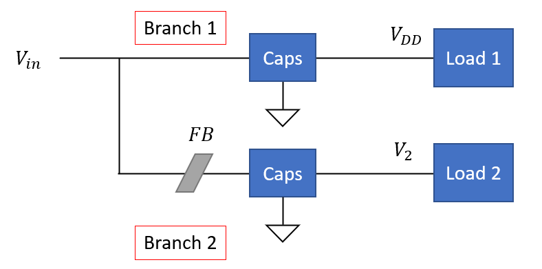
The idea here is to provide isolation between both branches at certain frequencies, meaning that we don't want Branch 1 to interfere with Branch 2. This works best when high capacitance is available in the Caps section in Branch 2; also small resistors (<1 Ohm) are typically used in series with FB and the caps in this filter. This also requires the noise created by Branch 1 does not overlap with the high transfer impedance region between the two branches (Z12). In other words, you're passing the power you want into Branch 2, but trying to block the noise from Branch 1.
What's the Verdict on the Ferrite?
Should you actually do this? It all depends, and this is all easier said than done. The addition of the ferrite bead does add to the transfer impedance between Branch 1 and Branch 2, and it increases the self impedance of Branch 2. My view is it should be avoided if you're working high frequency with a lot of IOs on Branch 2. If Branch 2 is just a low current, highly noise tolerant load (a PLL is not very noise tolerant!), then you might be okay, but you should simulate and test this first to be sure. I have seen one paper from DesignCon 2011 that shows how it significantly reduces jitter on a 3.125 Gbps SerDes PLL (see this link, Slide 21). To see the competing view where this technique might fail, read this article by Kella Knack.
Package Transfer Impedance
Just like a PCB can have transfer impedance between different rails in the PDN, components will also have transfer impedance between different terminals in the IC package. There is always a difficulty in getting the PCB's PDN self-impedance (diagonal elements) to be as small as possible due to the structure of PCBs and the inductance of small-case capacitors. In the PDN of a component package, the on-chip or in-package structure will include significant capacitance that sets low PDN impedance above about 1 GHz. This is what allows larger processors like FPGAs to pull power at very high frequencies for multiple high-speed protocols simultaneously without failing.
Just like packages have self-impedance, they also have transfer impedance. The transfer impedance exists between different dies in a package, or different I/Os in a die. However you choose to abstract these systems, the mathematical definition of transfer impedance also applies in packaging.
Power integrity and signal integrity problems can be difficult to solve, but you don’t need to be an expert in transfer impedance to solve your power and signal problems. The layout and routing tools in Altium Designer® are ideal for designing advanced electronics for high speed applications, and you’ll have access to an integrated SPICE simulation package to help you simulate power integrity, as well as determine an impedance matrix for your circuit. When you're ready to send your design into your manufacturer, use the Altium 365 platform to share your design files and stay productive.
We have only scratched the surface of what’s possible with Altium Designer on Altium 365. Start your free trial of Altium Designer + Altium 365 today.

About Author
Related Resources
Related Technical Documentation
Table of Contents
Design to Release, Without the Friction
- Keep reviews tied to the right version
- Reduce handoff confusion and rework
- Spot sourcing and release risk earlier
- Work solo, share when needed
Get Started
Thank you, you are now subscribed to updates.

