


Advanced Power Route Creation and Verification of Ground and Power Supply PCB Layout Traces with Altium Designer


Probably, the most formidable task of circuit board design is routing traces. In addition to connecting components accurately you must also route through vias for multi-layer PCB design while ensuring that spacing and clearance specifications meet the tolerances of your PCB fabrication and assembly services. And successfully meeting these challenges requires that you incorporate good grounding and power supply PCB layout into your design.
ALTIUM DESIGNER
The most advanced, comprehensive PCB design software package that simplifies power supply and ground trace layout.
Due to the pervasive use of digital and analog electronics in virtually all types of products, it is common to have power supplies resident on printed circuit boards or PCBs. These PCB designs typically contain DC-DC converters to lower an input voltage to a lower level to power transistors and integrated circuits (ICs). It is also common to have PCBs that combine digital and analog design as well as electronic circuits that require a mixed-signal design that includes high-frequency components. If your board contains a power supply circuit or needs to distribute power to its components then applying good power supply PCB layout guidelines is a must for safe, reliable operation and PCB manufacturing.
What is a Good Power Supply PCB Layout?
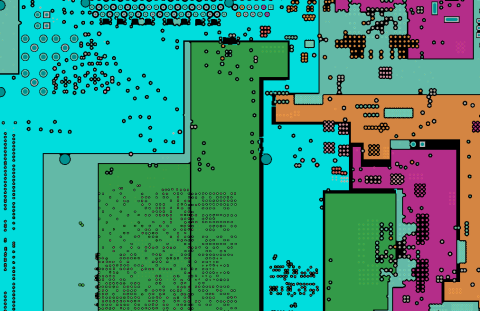
PCB design guidelines state good power supply in a PCB layout equates to the distribution of your power supply signal(s). This often is designed as a copper power plane that reaches all required devices, components, and circuits within an acceptable range or level that allows for the desired operation. All power signals require a return path; therefore, distribution also means that adequate paths to ground must also be supplied. To facilitate the manufacture of your PCB design, especially PCB assembly, your power and ground traces must adhere to the design for manufacturing (DFM) tolerances from your PCB manufacturer. Moreover, power supplies are usually high power devices and your design must include heat dissipation paths to thermal relief pads, as shown in Fig. 1 below, to prevent overheating during soldering that could damage components or the board.

Fig. 1 Creating a thermal relief
Different Signal Types Require Different Trace Routing Schemes
When designing the power and ground signal routing for your board it is important to follow good trace routing guidelines that recognize the necessity for isolating signals of different types to improve signal integrity. This should be reflected in your component layout which will make the isolation of trace routing schemes more straightforward.
- It is imperative that your board design separate analog, digital and high-frequency signals to prevent noise that can play havoc with circuit operation.
- Knowing where to place ground planes and how to route to them is important regardless of the size of your PCB stack-up.
- The manufacturability of your board may well depend upon your circuit’s ability to quickly dissipate heat.
Make Power Supply and Ground Routing Easy with Altium Designer’s ActiveRoute
There are many power supply PCB layout guidelines and considerations that a PCB designer must incorporate when routing traces; including trace widths, trace lengths, copper weights, and what type of vias to use for signal, power, and ground planes. When you add clearance and separation requirements, various power supply levels, mixed-signal processing, and obstacle avoidance trace routing can seem quite daunting. And without the right PCB software for routing it can be a long and tedious exercise before an acceptable PCB layout is realized that meets your operational and manufacturing mandates.
ActiveRoute Flexibility allows for Automatic, Manual and Interactive Trace Routing
To meet the many PCB design demands, which are at times in conflict, of route tracing you need a routing tool that can free you from having to juggle the restraints and recommendations that restrict your paths. However, you also need the flexibility to decide constraint priorities and make necessary geometric choices for routing around objects. For most PCB software design packages you must select either manual, auto-routing, or as is most often the case, apply them sequentially. This method of routing is time-consuming and usually requires extensive error correction. The solution is Altium ActiveRoute which lets you interactively take advantage of the consistency of automation and the creativity of manual routing.

Fig. 2 Route shaping options in Altium Designer
- For most designs, applying angles to route around components and drill holes is required. The shapes that you choose can make your board manufacture simpler or lead to problems.
Learn the best shapes and angles for routing around obstacles.
- Altium’s Active Route allows you to route multiple traces simultaneously, set fixed routing parameters, or change them on the fly.
- The ability to combine automated and manual routing is the best method for creating traces quickly and accurately.
Learn about Altium Designer’s advanced interactive routing functionality.
Altium Designer’s Advanced Capabilities Verify your PCB Layout Routing meets Performance and Manufacturability Requirements
Passing the Printed Circuit Board design rule checker (DRC) is a good indication that your PCB design meets the qualifications for your board fabrication and PCB assembly services, provided that good DFM in accordance with your contract manufacturer (CM) was utilized. However, before sending your design files off there are additional reviews of your power supply and grounding that should be performed; including visual inspection and thermal analysis.
3D Visual Inspection, Interactive Routing, and Power Distribution Network Analysis are the Tools you Need to Ensure the Best Power Supply and Grounding PCB Layout
The last stage of PCB layout design is verification. One part of verifying your design that should never be overlooked is the visual inspection. It is indeed possible that your PCB layout may pass all of the rules and restraints that you have instituted and not meet other requirements; such as placement of components or other elements due to the enclosure, mounting, or other concerns. Another important verification procedure is thermal analysis. With Altium’s Power Distribution Network (PDN) Analyzer you can simulate current flows along your traces to identify thermal dissipation issues.
- With Altium’s 3D capture you easily check all aspects of your PCB design graphically.
- It is much less time-consuming and cost-effective to simulate trace current flows to identify potential heat buildup issues during the PCB design where they can be easily fixed as opposed to discovering them after having a manufacturing run done.
Learn how to identify current flow issues with PDN Analyzer.
- Correcting power supply and ground trace errors can be easily corrected using Altium’s interactive routing capability.
Learn about Altium Designer interactive routing mode options.
The PCB layout of your grounding and power supply PCB design requires that you not only follow good trace routing guidelines that incorporate isolation of signal types and thermal reliefs but that you have a comprehensive PCB design package with functionality to help you reduce design time and avoid additional costs for corrections. For the best PCB traces and schematic captures, get the best Printed Circuit Board solution: Altium Designer with ActiveRoute.

About Author
Related Resources
Related Technical Documentation
Table of Contents
- What is a Good Power Supply PCB Layout?
- Different Signal Types Require Different Trace Routing Schemes
- Make Power Supply and Ground Routing Easy with Altium Designer’s ActiveRoute
- ActiveRoute Flexibility allows for Automatic, Manual and Interactive Trace Routing
- Altium Designer’s Advanced Capabilities Verify your PCB Layout Routing meets Performance and Manufacturability Requirements
Design to Release, Without the Friction
- Keep reviews tied to the right version
- Reduce handoff confusion and rework
- Spot sourcing and release risk earlier
- Work solo, share when needed
Get Started
Thank you, you are now subscribed to updates.


