
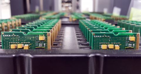


Preventing Top DFM Errors in Your PCB Design

At a Glance
Get a manufacturer's view on the most common DFM errors in your PCB design and what you can do about them.


Every circuit board should obey DFM (design for manufacturability) guidelines to avoid potential manufacturing and assembly errors. This also focuses on cost reduction, quality improvement, and defect-free manufacturing. In this article, we will explain some of the top DFM errors in PCBs and various techniques to avoid them.
A Glance at PCB Design for Manufacturing (DFM)
DFM analysis allows manufacturers to review the design of the board from various aspects to modify its materials, dimensions, and performance most efficiently. It detects the design issues instantly and rectifies them well in advance of production. A step-by-step approach to design for manufacturability analysis consists of the following attributes:
- Identification of design violations that will affect the manufacturing process.
- Determination of the precise manufacturing process according to the geometry and material requirement.
- Inspection of the board design and determining if the specification will align with the finished product.
- Selection of materials (as per properties, physical strength, and texture) that depend on the board’s dimensions.
- Ensuring the design follows regulatory compliance to fulfill quality standards and reliability.
Top DFM Errors
The commonly found DFM issues include slivers, annular ring breakouts, acid traps, etc. Let’s have a look at the common violations and their prevention.
Prevention of Slivers
Slivers are small wedges of dry film resist that expose copper and create shorts. They can either be conductive (copper) or non-conductive (solder resist). There are two reasons that lead to the formation of slivers. The first case is when a long, thin feature of the copper or solder mask is etched away. Slivers that detach cause shorts during fabrication. In the second case, slivers form by cutting a section of a board design too closely or too deeply. A circuit board's functionality can be adversely affected by this.
Solution:
Implement a minimum photoresist width to avoid this defect. Apply the same net spacing (less than 3 mils) or airgap that can be removed or filled. A proper DFM analysis is necessary to identify possible areas where slivers could form and resolve issues if any.


Component Selection
Component selection should be done based on its availability, lead-time considerations, and monitoring of obsolete parts. This ensures components are available well before the commencement of manufacturing.
Determine the sizes of components and packages by properly studying the BOM. You can opt for larger components for resistors and capacitors when sufficient space is available. For instance, use a 0603 or 0805 size capacitor/resistor instead of a 0402/0201. The selection is influenced by voltage, current, and frequency. When possible, choose smaller packages; otherwise, select larger ones. Overuse of small component packages can complicate circuit board assembly, thereby making cleaning and reworking more difficult.

Test Points
DFM includes test points for all important signals to check the electrical connectivity after building the board. If excluded, it will be difficult to check the final product. Here are a few pointers to avoid possible manufacturing issues:
- For ease of testing, place all test points on the same side of the board.
- Keep a minimum distance of 0.100 inches between the test points to increase the test's effectiveness.
- Designate the area for taller components.
- Circulate all the test points evenly for easy access with multiple probes.
- Design your layout keeping manufacturing tolerances in mind.
Vias and Drill-to-Copper
Drill-to-copper is the distance from the edge of a drilled hole to the nearest copper feature. But PCB designers consider drill-to-copper from the finished hole size (FHS) to the nearest copper feature.
Designers should always consider the drilled diameter (FHS + drill tolerance) to determine the correct distance. The drilling diameter can be determined from the below equation:
Finished hole size + tolerance = drill diameter
Normally, the distance should be 5-8 mils but it depends upon the layer count. Board layout tools do not have any particular design rule checks (DRCs) for drill-to-copper. However, if you use adequate spacing in your design, you can have a clearance of 8 mils. This is the most important attribute to consider while doing DFM analysis.

In annular rings, tangency or breakout can occur when the drill bit fails to reach the desired spot and shifts away in the same axis. This causes marginal interconnections and affects reliability.

Here are a few tips to avoid DFM problems that occur during drilling:
- Incorporate wide annular ring areas in your design by adapting bigger pad sizes. It ensures good conductivity and ease of drilling vias in the middle of the pad.
- Verify whether the plated drills have copper pads on all copper layers.
- Sierra Circuits recommends a minimum of 8 mils of drill-to-copper.
- Maintain a minimum aspect ratio to prevent misregistration of the drill.
- Define the drill type (PTH/NPTH) and drill count/size.
- Make sure the copper features and drills fit inside the profile of the board.
- Design an annular ring greater than or equal to the minimum annular ring size (4 mils) that can be manufactured by the vendor/fab house.
- Add teardrops to prevent annular ring breakout in complex designs and smaller annular rings.
Number of Drills Should Match the Drill Chart
It is crucial to match the number of drills with the drill chart. A drill chart is included in the fab drawing. Sometimes the drill chart doesn’t match with the actual drill count. In that case, you will need to modify or regenerate the drill chart.

As a simple design point, try to minimize the number of different drill sizes used in the PCB layout. It's best to pick one or two via sizes that can handle most of the layer transitions for signals and possibly a few others that will be used for mounting holes or non-plated holes.
Clearances
There are three types of clearances to observe in DFM analysis.
Edge clearance:
Many designers forget to provide adequate clearance between copper and the edge of the PCB. The proximity of copper to the edge can create shorts between adjacent layers if the current is applied to them. This is a result of exposed copper around the perimeter of the board. It is possible to resolve this problem by adding clearance to the design. Check the following approximations:
- For outer layer: 0.010”
- For inner layer: 0.015”
Line spacing:
Line spacing is the minimum distance between two conductors. It depends on materials, copper weight, temperature variations, and applied voltage. It also depends upon the capabilities of the manufacturer.

Solder mask clearances:
- Keep solder mask clearance greater than solder pads, except in the case of solder mask-defined pads.
- The best way to prevent solder bridges is to extend the mask opening onto the copper pad or provide barrel relief (solder mask clearance = drill size + 3 mils).

Missing Solder Mask
Sometimes, the solder mask may be partially or entirely absent between the pads. This exposes excess copper, leading to solder bridges and shorts that compromise board performance. This happens when the solder mask is not defined or when settings from a larger board are applied to a smaller board, leading to large pad holes.

Follow these design tips for solder masks:
The relative size of the solder mask should be 4 mils larger than the feature size.
Keep solder mask width/bridge to a minimum of 4 mils.
Maintain the space between the edge of the copper feature and the edge of the solder as 2 mils.
Acid Traps
Another DFM error to watch out for is an acid trap. An acid trap is basically any design that incorporates acute angles that will attract acid concentrations to that area. This may result in over-etched traces and open circuits as a byproduct of the acid traps.

Avoid laying the traces coming to the pads at acute angles. Place the traces at 45° or 90° relative to the pads. Verify that none of the trace angles have created acid traps after routing the traces.
Silkscreen Checks
Silkscreen check involves the different attributes that will influence the DFM analysis and will prevent possible errors. Here are a few important guidelines:
Orientation: Silkscreen may sit on the pads, and this should be checked by running a DRC. Silkscreen could also overlap a via hole, although this is acceptable if the vias are tented. This can happen while rotating the text and adjusting the component reference designator marks. Trim the reference designator marks that go over pads and vias to prevent overlapping.

Line width and text height: We recommend a minimum line width of 4 mils and text height of 25 mils for easy readability. Always use standard colors and larger shapes for good representation. Typically, the size should be 35 mils (text height) and 5 mils (line width). If the board is not dense and there is sufficient space for large text use the following size:
|
|
|
|
|
|
|
|
In case the above specifications do not work for a medium-density board, use the following size:
|
|
|
|
|
|
|
|
When the above size does not work, refer to the following: For a medium-density board:
|
|
|
|
|
|
|
|
Silkscreen printing method: The specific method influences many design parameters such as size, clearances, etc., and elements like pads, vias, and traces. Specify these according to manual silkscreen printing, liquid photo imaging, and direct legend printing.
Prioritizing markings: Prioritize the silkscreen marking as per the classification: regulatory requirements, manufacturer identification, assembly aids, and testing aids.
Following design for manufacturability guidelines helps you recognize errors in the early design stage. Fortunately, the DRC engine in Altium Designer® can help you catch these problems before you go to production. After you consult with your manufacturer, you can program the constraints listed above into your PCB design rules to ensure you can quickly catch and correct errors. Once your design is ready for a thorough design review and manufacturing, your team can share and collaborate in real-time through the Altium 365™ platform. Design teams can use Altium 365 to share manufacturing data and test results, and design changes can be shared through a secure cloud platform and in Altium Designer.
We have only scratched the surface of what’s possible with Altium Designer on Altium 365. Start your free trial of Altium Designer + Altium 365 today. And make sure to visit the Sierra Circuits website to learn more about manufacturing and assembly processes.

About Author
Related Resources
Table of Contents
Design to Release, Without the Friction
- Keep reviews tied to the right version
- Reduce handoff confusion and rework
- Spot sourcing and release risk earlier
- Work solo, share when needed
Get Started
Thank you, you are now subscribed to updates.


