Use the Best RF Design Software for High Frequency PCBs

Designing radio frequency systems to support high frequencies and digital interfaces is challenging and requires the best RF design software tools. RF engineering in a high GHz band takes the best RF design software to ensure accurate PCB trace routing, layer stack design, and circuit design. Use Altium Designer for your RF design process and to take your next GHz band system to manufacturing.
ALTIUM DESIGNER
A unified PCB design software application with circuit design features, a powerful PCB editor, and simulation features for RF engineering professionals.
Many electronics engineers are familiar with digital design concepts, but what about the peculiarities of RF design? The field is sometimes called "black magic" and for good reason, as so much of the discipline requires studying and understanding electromagnetism at a deep level. For the RF designer, they need a particular set of design features that can help them model their systems as well as transfer designs into a PCB layout. They also need full control over their design documentation to ensure their designs will be manufactured to specification.
Designers that use the best RF design software can perform a variety of system level simulations at the circuit level, as well as build a PCB layout for their new device. A platform like Altium Designer gives users total control over their RF designs through simulation tools inside the schematic, post-layout simulations for crosstalk and reflection simulation, a layer stack manager for building a circuit board, and integrations with other design tools. When you need to design an RF PCB to support systems operating at any frequency, from GHz bands to mmWave, use a comprehensive design platform like Altium Designer, the industry’s best digital, RF, and mixed-signal design software.
Accurate System Design and Simulation in RF Engineering
Every new electronic system will start as a circuit design, and electronics engineers need powerful design and simulation tools to build and qualify RF systems. The best RF circuit design software should provide a set of simulation tools for circuit simulation that go beyond the generic components found in typical SPICE simulation applications.
- An integrated SPICE simulation engine
- Import simulation models extracted from other programs
- Matching circuit design with access to real components
- Footprint creation for printed components and assignment to components in component libraries
As an example, consider a standard printed devices like a Wilkinson divider or a coupler. These devices can be represented in a schematic in your PCB design software as a multi-port schematic symbol. In an external field solver program (such as CST, Ansys, Simbeor, etc.), it's possible to extract the equivalent SPICE subcircuit model for these devices. These equivalent SPICE models can then be saved in a standard model format (MixedSim, LTSpice, PSpice, etc.). After saving a model, the symbol and footprint for the printed component can be designed, and the simulation can be attached to the component in a schematic sheet.

Any of these components that have a model attached can be used in a SPICE simulation to evaluate system functionality.
Resources for RF Design
Altium Designer includes the best schematic editor that gives access to a huge range of real components with simulation models for use in RF circuit design and analysis. Designers can streamline the RF design process while also aiding systems-level design and analysis. It’s simple to create components in your schematics for evaluation and simulation with Altium Designer’s complete set of component creation tools and simulation features. Like other SPICE-based simulators, Altium Designer also helps you work with mixed-signal systems in RF engineering.
- RF circuit design involves many front-end tasks, including impedance matching network design, filter design, footprint creation for a physical PCB layout, and much more.
- Printed RF circuits can require unique SPICE models that are extracted from external field solvers or modeling applications. Altium Designer supports these models inside the integrated SPICE simulator and component libraries.
Learn more about support for 3rd party simulation models in Altium Designer.
- Altium Designer’s integrated design environment makes it simple to create and run SPICE simulations.
Learn more about running SPICE simulations in Altium Designer.
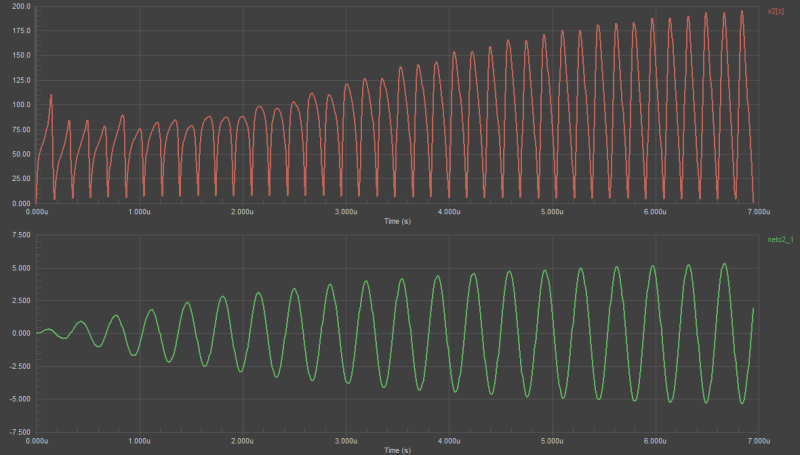
Transient analysis of RF circuit designs and other simulations are streamlined in Altium Designer’s schematic editor.
RF PCB Layout With the Best RF Design Software
Once components are designed, schematics are completed, and the system functionality is simulated, your RF design software should aid physical PCB layout with a world-class PCB Editor. The complete set of routing and component layout tools in Altium Designer will help you place components, route transmission lines, and ensure conformance to design rules in a single application.
With a powerful set of routing features, you can ensure impedance matching in transmission lines with design to low insertion loss in your PCB traces. You’ll have full control over your PCB layout, as well as powerful verification features in a single RF design software application. The verification features you need in RF design software are available for specific nets or groups of nets in Altium Designer, as well as in 3rd-party applications. Altium Designer gives you access to both sets of verification tools to help ensure your physical layout matches the functionality you expect from your system design.
Post-Layout Simulations and 3rd-Party Electromagnetic Field Solvers
After you complete the PCB layout of your RF design, it’s important to put the design through a round of simulations to ensure any RF signal integrity problems are solved or prevented. Altium Designer includes a set of post-layout simulation tools that can be used to reflection and crosstalk analysis, as well as impulse response analysis by designing a short input pulse in the stimulus tool. The simulation tool in Altium Designer operates inside the PCB Editor on a net-by-net basis to help you speed up design verification before prototyping.
For work in 3rd-party simulators, Altium Designer can be used to export your design data into multiple formats that are used by industry-leading electromagnetics tools.
- STEP and Parasolid models
- IDF models (EMN/EMP)
- Ansys EDB exports
- ODB++ for PCB-specific simulators
These tools have come together to streamline the high-frequency RF design process with powerful design, layout, and simulation features. Altium Designer includes an additional set of simulation tools to help you verify your design before manufacturing.
- Altium Designer makes it easy to send your design into Ansys simulation software and electromagnetic field solvers with its EDB Exporter extension.
- Designing to GHz band radio frequencies can be difficult without the right set of PCB design and analysis tools.
Learn more about GHz band radio frequency designs in Altium Designer.
- RF interference and emission of electromagnetic waves are persistent problems in RF PCB design and analysis. You can solve many of these problems with the right PCB stackup.
Learn more about designing a PCB stackup for low noise in Altium Designer.

RF Design Software That Gets You to Manufacturing
Altium Designer doesn’t stop with RF circuit design and layout tools. After using integrated and 3rd party simulation features, RF designers can quickly prepare their board for manufacturing in standard processes. It’s never been easier to prepare a new RF design for high-volume manufacturing, including advanced high-frequency RF designs. You can take advantage of the following manufacturing features in Altium Designer:
- Gerber file generator in the latest file formats (RS-274-X and X2)
- Fabrication and assembly drawing generation with the Draftsman utility
- Bill of materials generation with automated supply chain checking
- NC drill file, pick-and-place file, and netlist generation
Altium Designer’s major advantage over other RF design software platforms and PCB design applications comes from its integrated design environment. Everything you need for RF circuit design, PCB layout and transmission line routing, and post-layout simulation is included in a single application. Altium Designer helps you stay productive and design cutting-edge technology with the industry’s most powerful PCB design application for product development.
Experience Rules-Driven Design in Altium Designer
The rules-driven design engine in Altium Designer unifies every design tool you need into a single application. When you need to create a high-frequency analog system or mixed-signal PCB, the rules-driven design tools in Altium Designer keep you productive and ensure your design meets your application requirements. Best of all, you won’t have to use external programs for RF filter design, simulation, and impedance control; everything you need can be found in Altium Designer.
- Altium Designer is a complete RF design software application for low and high-frequency systems and RF circuits. Access everything you need for high-quality RF PCB designs in Altium Designer.
Learn more about the integrated design environment in Altium Designer.
- Altium Designer’s integrated field solver from Simberian gives RF designers an integrated toolset for ultra-accurate propagation delay and impedance calculations.
Learn more about the integrated field solver from Simberian in Altium Designer.
- When you’re ready to share your circuit board with other PCB designers or your manufacturer, Altium 365 lets you instantly share your design and production data through Altium Designer or on the web.
Learn more about sharing your PCB project data with Altium 365.

Stop using separate programs for RF PCB layout, RF circuits design, simulation, field solvers, and analysis. Instead, take control over all aspects of your RF PCB layout with the complete set of PCB design tools in Altium Designer. Only Altium helps you stay at the cutting-edge of technology while helping you collaborate and stay productive.
Altium Designer on Altium 365 delivers an unprecedented amount of integration to the electronics industry until now relegated to the world of software development, allowing designers to work from home and reach unprecedented levels of efficiency.
When you’ve finished your design, and you want to release files to your manufacturer, the Altium 365™ platform makes it easy to collaborate and share your projects.
We have only scratched the surface of what’s possible with Altium Designer on Altium 365. Start your free trial of Altium Designer + Altium 365 today.

