

Signal and Power Integrity: The Hidden Forces Behind Reliable Modern Electronics

Modern electronic products are pushing the limits of speed, density, and complexity. High‑speed interfaces are everywhere, power rails are more demanding, and timing margins are tighter than ever. In this environment, Signal Integrity (SI) and Power Integrity (PI) have become essential pillars of successful PCB design.
They determine whether a product performs reliably, passes compliance, and reaches the market on schedule. When they’re overlooked, the consequences ripple across engineering, manufacturing, and the business as a whole.
What Signal Integrity Really Means
Signal integrity is the practice of ensuring that electrical signals travel through a PCB cleanly and accurately. It’s about designing transmission paths that:
- Move data reliably from point A to point B
- Minimize signal degradation
- Prevent unwanted interference
When SI problems creep in, they show up as:
- Reduced performance
- Higher error rates
- Compliance failures
- Increased power consumption
- Unpredictable or intermittent behavior
- Poor user experience
And the financial impact can be significant. Late‑stage fixes, additional testing, and extra prototype spins add cost and delay. A single PCB prototype can cost thousands of dollars, and each redesign compounds the risk of missing critical market windows.
Power Integrity: The Other Half of the Equation
Power integrity focuses on delivering clean, stable power to every component on the board. As supply voltages shrink and current demands rise, maintaining a robust power delivery network becomes increasingly challenging.
Poor PI can lead to:
- Voltage drop
- Excessive noise
- Timing instability
- EMI issues
- Field failures
A power analyzer helps designers evaluate:
- DC drop across power nets
- Current density
- Power plane impedance
- Transient response
- Thermal and reliability concerns
SI and PI are deeply interconnected. A noisy power rail can distort high‑speed signals, and poorly routed signals can inject noise into the power system. Treating them as separate problems is no longer practical.
Why Traditional SI/PI Workflows Slow Teams Down
In many organizations, SI and PI analysis still follow a legacy workflow:
- The PCB designer completes layout
- A specialist imports the design into external tools
- The specialist verifies data, configures simulations, and interprets results
- Feedback is sent back to the designer
- The design is revised
- The loop repeats
This approach is:
- Slow
- Expensive
- Dependent on scarce experts
- Disconnected from the design environment
- Prone to late‑stage surprises
It also reduces designer autonomy and creates bottlenecks that are difficult to scale as teams grow or projects become more complex.
Integrated SI/PI Analysis: A Smarter, Faster Approach
Embedding SI and PI analysis directly into the PCB design environment transforms the entire development process.
Proactive Risk Reduction
Issues are caught early, long before they become costly problems.
Improved Development Efficiency
Shorter feedback loops keep projects moving smoothly.
Lower Costs
Fewer prototype respins and compliance retests reduce overall development expenses.
Scalability and Consistency
Standardized, in‑design analysis ensures repeatable quality across teams and projects.
This shift isn’t just a technical improvement — it’s a strategic advantage.
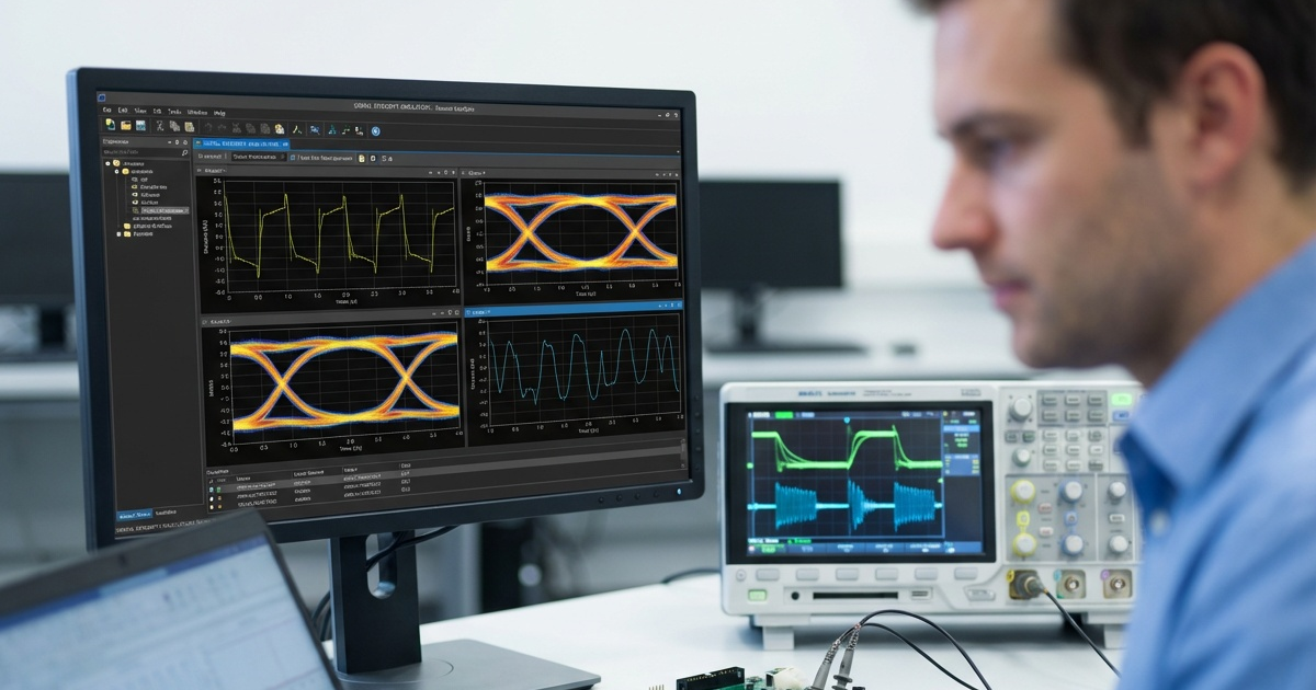
Design‑Time Signal Analysis in Altium Designer
Modern tools now bring SI analysis directly into the PCB editor. One example is the Signal Analyzer extension, which provides:
- One‑click analysis and immediate feedback
- Impedance analysis and detection
- Delay calculation
- Insertion and return loss evaluation
- Probing and image capture
- Expert‑guided reporting
- Shareable results for collaboration
This empowers designers to identify and resolve SI issues as they work, rather than waiting for external reviews.
Extending the Same Power to Power Integrity
The same philosophy applies to PI. When PI analysis is integrated into the design environment, designers can evaluate:
- DC drop
- Current density
- Power plane impedance
- Weak power delivery paths
- Decoupling capacitor effectiveness
This creates a unified workflow where SI and PI are treated as first‑class design considerations rather than afterthoughts.
The Future of PCB Design
As electronics continue to evolve, SI and PI will only grow more critical. Integrated analysis tools give teams the ability to design with confidence, reduce risk, and deliver higher‑quality products faster.
Organizations that embrace in‑design SI and PI analysis will consistently outperform those relying on outdated, specialist‑only workflows. The result is better products, fewer surprises, and a smoother path from concept to market.
About Author
Related Resources
Related Technical Documentation
Table of Contents
- What Signal Integrity Really Means
- Power Integrity: The Other Half of the Equation
- Why Traditional SI/PI Workflows Slow Teams Down
- Integrated SI/PI Analysis: A Smarter, Faster Approach
- Design‑Time Signal Analysis in Altium Designer
- Extending the Same Power to Power Integrity
- The Future of PCB Design
Get the Full Signal Analyzer Experience
- Turn SI analysis into fast, coordinated decisions.
- Your Agile Teams evaluation includes full access to Signal Analyzer.
Contact Us
Thank you, you are now subscribed to updates.