Microstrip Impedance Calculator

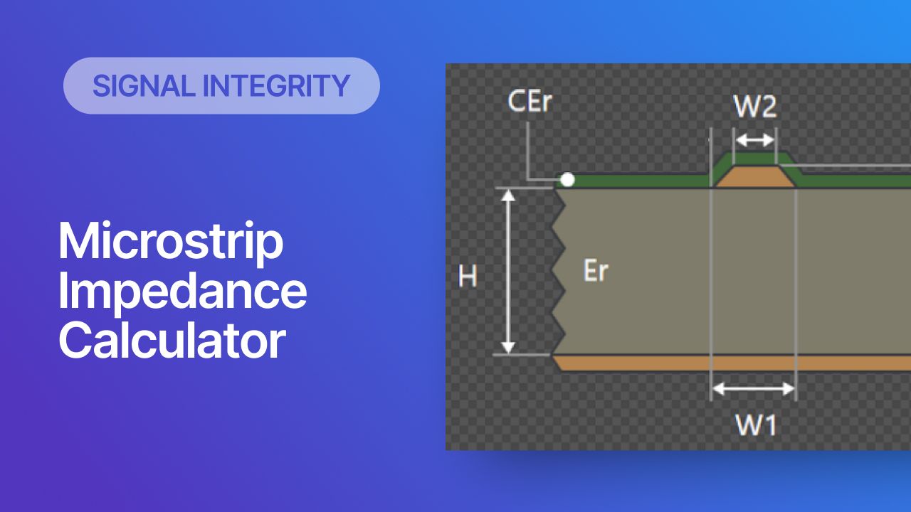
Microstrips are one common routing style used in mid-range frequency applications like sub-1 GHz radios, as well as higher speed buses with signal-ended signals (e.g., DDR). If you need to find and use an efficient and accurate microstrip impedance calculator that provides lossless impedance values, you can use our free tool below. This microstrip impedance calculator gives you a good start for estimating the trace width and PCB dielectric thickness that will produce a target impedance value. Make sure you use an accurate tool like this before you start building your stackup as this can help you identify the best laminate materials to use for your target impedance and trace width.
How to Use a Microstrip Impedance Calculator
Most of the microstrip impedance calculators you’ll find online use a similar process: enter your microstrip geometry and Dk value for your PCB substrate materials, and the tool will return the impedance for your microstrip trace. As you adjust the width of the line, you can eventually get the microstrip impedance calculator to converge on the desired impedance value, and you have finished designing the microstrip trace.
Note that some online microstrip impedance calculators will determine the width for a given target impedance, copper weight, and substrate thickness. These other calculators will just use the IPC-2141 formulas that are solved for the trace width. The results are known to be inaccurate, especially when one examines the effective dielectric constant predicted with these calculators. However, the microstrip impedance calculator provided here uses a more accurate, but more complex, set of equations for trace impedance.

Results
The microstrip impedance calculator shown above uses Wadell’s equations for microstrip impedance, which can be found in the seminal textbook Transmission Line Design Handbook. These equations are relatively simple compared to other transmission line geometries, comprising only 2 interrelated equations for the microstrip impedance and effective dielectric constant. The resulting impedance value is known to be highly accurate over a broad range of frequencies spanning well beyond 1 GHz.
For differential pairs of microstrips, the formulas involved are much more complicated because coupling between the traces in the differential pair must be included in the impedance calculation. This makes the problem of determining impedance much more complex, and building an initial lossless model requires a larger set of formulas from Wadell’s textbook or an electromagnetic field solver. If you need to use differential microstrips, we have another differential impedance calculator that can give you a highly accurate estimate of differential microstrip impedance.
Microstrip Impedance Calculators Don’t Include Some Data
When you need to get an initial estimate of trace width required for a target impedance, then trace calculator tools are very useful can they can help your understand how your substrate materials will affect the impedance of a trace. However, there are many important pieces of information that aren’t included in online microstrip impedance calculators:
- Losses - Almost every online PCB impedance calculator will completely ignore losses, or they simply produce a geometry-independent value for attenuation based on loss tangent, which is incorrect. The trace geometry and roughness of copper foils used in PCB layer stacks are also important. Learn More.
- Dispersion - Geometric dispersion is included in the formulas, but not dielectric dispersion due to variations in the dielectric constant with frequency. Learn More.
- Solder mask - While losses in the solder mask can be included in a PCB transmission line impedance calculation, the resulting formulas are very complex and are difficult to use in a impedance calculator application. Learn More.
- No etch factor - Etching causes traces to be somewhat trapezoidal on the finished board, which will cause the real trace to have a different impedance. Etch compensation is normally applied during front-end engineering to help correct this imbalance. Learn More.
- No propagation delay - The propagation delay value for a PCB transmission line will always contain some loss, but this is not captured in simple online impedance calculators, or if they do it’s estimated from an incorrect formula. Learn More.
Use a Layer Stack Tool With a Built-in Field Solver
Obviously, there is a lot that goes into estimating microstrip impedance. Improving the results and producing more accurate models requires manually modifying the lossless impedance model by adding back in the skin effect/roughness impedance, or you must solve Maxwell’s equations directly. While the latter approach is more accurate in an arbitrary geometry, this requires a field solver or a numerical model that is extracted from field solver results.
The advanced PCB layer stack management in Altium includes a field solver that calculates impedance for common geometries, including microstrips, striplines, coplanar lines, and differential lines. These features are accessed in the layer stack management utility inside the PCB Editor in Altium. Simply click the Impedance tab and create a new calculation, and then create a design rule based on the impedance calculation results. The only thing you need to know to get started is the dielectric constant of your substrate materials.

The stackup design features in Altium can help you quickly get an accurate microstrip impedance calculation from a library of materials, or from totally custom materials with known material constant values. When you’re ready to release these files to your collaborators for more advanced simulations, Altium makes it easy to collaborate and share your projects. Everything you need to design and produce advanced electronics can be found in one software package.


