PCB Transmission Line Impedance Calculators

High speed designs won’t operate properly without an accurate calculation of transmission line impedance. Traces that support fast edge rate signals will act like transmission lines, even when their lengths are short. Best practices in high speed design dictate that, at minimum, traces be designed close to the required impedance to ensure minimal return losses.
To get an accurate impedance result, you could always calculate the impedance by hand, but the most accurate impedance formulas are very unwieldy to use by hand. To help designers get started with floorplanning, we’ve compiled a set of transmission line impedance calculators that implement the most accurate analytical formulas. Once you’ve determined an initial estimate of the trace width you’ll need for accurate impedance, you can go a step further and use the best stackup editor with a built-in impedance calculator to determine your required trace width.
How Transmission Line Impedance Calculators Work
Transmission line calculators all operate on similar principles: determine an impedance value for a particular transmission line geometry. In terms of how these calculators work, the impedance of a transmission line in a PCB can be calculated in four ways:
- Use the R, L, C, G parameters from the Telegrapher’s equations to calculate the impedance of the transmission line
- Build a model from experimental data of impedance vs. trace geometry, and use this to calculate impedance
- Use an analytical technique that provides lossless dispersionless impedance from Maxwell’s equations, such as Wheeler’s method as used in Wadell’s equations
- Use a field solver to numerically solve the electromagnetic field from Maxwell’s equations, then use the field to determine impedance
Transmission line impedance calculators, such as those you might find online, use #2 (for IPC-2141 based calculators) or #3 (for more accurate calculations from first principles). If you don’t have access to a field solver, taking the approach with #3 above will give you the most accurate results as long as you have the right calculator application.
The set of transmission line impedance calculators below implement method #3 to provide reasonably accurate results into the low GHz range. The pages linked below give you access to a free calculator you can use to get a reasonably good estimate of transmission line impedance before you use a more advanced application.
Four Free Impedance Calculators
The impedance calculators below are completely free to access and use. These calculators will return an impedance value for pairs of trace width, substrate thickness, and copper weight values. To use these to design for a target impedance, simply cycle through various geometric values for the trace width until the calculator returns the target impedance.
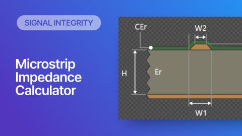
- Microstrip Trace Impedance Calculator
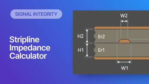
- Stripline Trace Impedance Calculator
- Differential Trace Microstrip Impedance Calculator
- Differential Trace Stripline Impedance Calculator
The standard geometries that are supported by these trace impedance calculators are shown in the graphic below. These transmission line arrangements are standard trace geometries implemented in PCB design software. If a coplanar arrangement is selected, you can approximate this trace routing style by setting at least approximately 10 mils, as long as the dielectric thickness is ~10 mils or less.

The models used in these transmission line impedance calculators are based on Wadell’s equations, which are known to provide highly accurate lossless impedance values. While they are not perfectly accurate due to certain factors in real materials, they are useful for getting a quick estimate of trace impedance for the above geometries. The main factors that will limit the accuracy of impedance calculators at progressively higher frequencies are:
- Copper roughness
- Dielectric losses and dispersion
- Parasitics, specifically parasitic capacitance
Once your operating frequency becomes too large, the result you get from a calculator like those linked above will not match the real values you’ll find on a PCB. For a digital signal, this refers to the case where the rising edge of a signal on the transmission line becomes very fast and most of the signal content becomes concentrated in the GHz range. For RF signals, this becomes important into the higher GHz range (above 5.8 GHz Wifi). The video below outlines some of the factors that cause PCB trace impedance calculators to experience lower accuracy at higher frequencies.
Get Greater Accuracy With Altium’s Layer Stack Manager
The calculators shown above are a great start to help you quickly determine an approximate trace width needed to hit your target impedance in your layer stack. However, even the highly accurate analytical formulas used to build those calculators have their limits above a certain frequency range. This is where you should use a more advanced tool inside your PCB editor to create your layer stackup.
To get much more accurate results, use the Layer Stack Manager in Altium Designer®. This utility comes standard inside the PCB Editor in Altium Designer and it includes a built-in electromagnetic field solver for impedance calculations. The impedance tool provides highly accurate impedance results for single-ended, differential, and coplanar transmission line arrangements, including asymmetric striplines. The results can then be applied to nets or groups of nets as a design rule to ensure consistent impedance throughout your interconnects.
Altium Designer includes everything you need to design advanced electronics with high speed digital signals and RF signals. Once you’ve completed your high speed PCB and you’re ready to share your designs with collaborators or your manufacturer, you can share your completed designs through the Altium 365™ platform. Everything you need to design and produce advanced electronics can be found in one software package.
We have only scratched the surface of what is possible to do with Altium Designer on Altium 365. Start your free trial of Altium Designer + Altium 365 today.


