Stripline Impedance Calculator

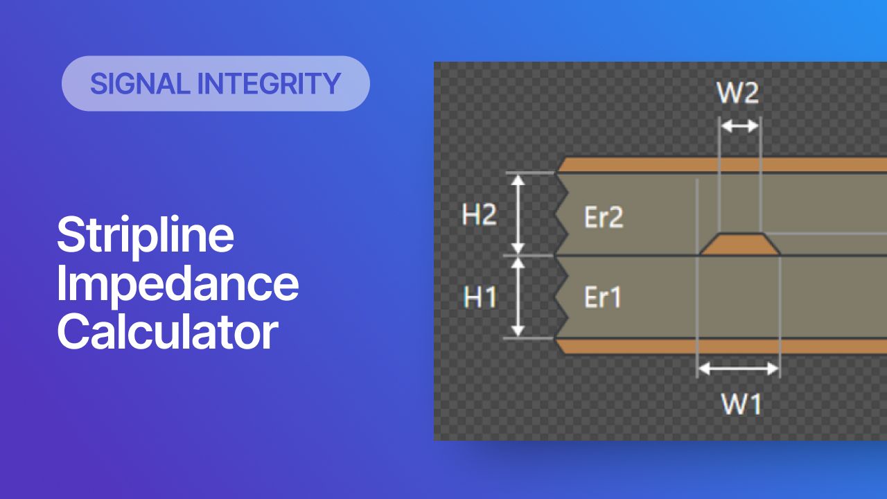
Striplines provide some advantages over microstrips as they take advantage of natural shielding and coupling from nearby ground plane layers. Although they tend to experience higher losses due to total confinement in the dielectric, they can be thinner due to the high dielectric constant used in internal layers of a PCB. A stripline impedance calculator can help you determine the width that will be needed to hit a target impedance for a given substrate dielectric and thickness. The free impedance calculator shown below can help you determine the correct width needed to hit a target impedance.
How to Use a Stripline Impedance Calculator
The stripline impedance calculator provided below is useful for gaining an initial estimate of trace impedance for striplines. The calculator is set up to handle an asymmetric arrangement, where traces are not centrally located in the PCB layer stack. The required inputs are the Dk value for the dielectric constant of the PCB substrate, and the thickness of the dielectric material between the PCB ground planes.
Like many other calculators you’ll find online, the stripline impedance calculator shown below returns an impedance for a given trace geometry. It will not do the inverse calculation as this requires solving a complex numerical equation that does not, in practice, have an analytical solution. To use the calculator below, you must enter an initial trace width, dielectric thickness, copper foil thickness, and dielectric constant. After entering this information, adjust the trace width until the impedance reaches the targeted value.

Results
This calculator tool includes everything needed to calculate the lossless impedance of a stripline. Asymmetric and symmetric versions of a stripline can be implemented with this calculator application. The calculator produces more accurate results than the IPC formulas for impedance because it implements a more accurate model that is not based on a limited dataset. Instead, the above calculator implements Wadell’s equations for stripline impedance, which can be found in his textbook Transmission Line Design Handbook.
Drawbacks of Online Impedance Calculators
Analytical impedance calculators are excellent tools for getting an initial estimate of trace impedance based on a specific set of dielectric materials implemented in the PCB stackup. However, when we look to the more advanced case where high frequency effects begin to dominate, or when lossy dielectrics are used throughout the PCB stackup, it will be necessary to consider additional effects that impact the impedance calculation. Analytical impedance calculators are missing some important information that is needed in more advanced impedance calculator applications.
- Dispersion - Dielectric constants in PCB substrate materials will be some function of frequency, meaning different frequencies can experience different impedance and losses. This is why calculators will not ask for an operating frequency value; they cannot do anything to account for dispersion in their models. Learn More.
- Loss tangent - Very few impedance calculators you’ll find on the internet can account for losses. Most applications simply ignore losses from dielectric absorption, copper roughness, and radiation. Learn More.
- No etch factor - The etching profile along the length of the trace will cause the impedance to deviate from its target value, and analytical calculators would need a much more complicated model to account for etching. Learn More.
- No propagation delay - The propagation delay depends on the dielectric properties, location of the trace in the PCB stackup, and the presence of nearby ground. Most impedance calculators will just give the value from the IPC-2141 standards, which is an incorrect value. Learn More.
- Solder mask - Solder mask materials create additional loss and they modify the propagation constant along propagation direction. Online impedance calculators will ignore the solder mask as analytical models for coated traces contain many complicated equations. Learn More.
Use a Layer Stack Tool With a Built-in Field Solver
To get around the above drawbacks of typical stripline impedance calculator applications like the one shown here, some more advanced methods are needed to determine impedance. As these additional effects are included in a transmission line model, the resulting impedance equations become very complex. Either a designer needs to solve Maxwell’s equations directly with a numerical procedure, or must manually apply corrections to a lossless model by adding back in the skin effect/roughness impedance.
Altium's PCB Layer Stack Management includes a field solver that provides highly accurate stripline impedance results, including for fully asymmetric stripline configurations. To access this utility, simply open your layer stackup in the PCB Editor and click on the Impedance tab. Once an impedance calculation is created, the results can be enforced in the PCB layout as a design rule so that the required trace width will be applied during routing. The only piece of information you need to get started is the dielectric constant (real and complex parts) of your substrate materials.

The stackup design features in Altium can help you quickly get an accurate stripline impedance calculation from a library of materials, or from totally custom materials with known material constant values. When you’re ready to release these files to your collaborators for more advanced simulations, Altium makes it easy to collaborate and share your projects. Everything you need to design and produce advanced electronics can be found in one software package.


