


The Best Tools for Multi-Board PCB Systems Design

At a Glance
Discover the best tools for multi-board PCB system design. Learn how to manage connectivity, EMC, 3D assembly, and design synchronization for complex projects.


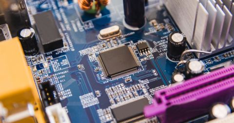
The design of multi-board PCB systems is a complex undertaking, necessitating that engineers effectively manage board-to-board connectivity, electromagnetic interference (EMI), signal routing, and mechanical integration. Best PCB design software incorporates functionalities such as inter-board connectivity verification, cable harness design, and mechanical collaboration tools to address these challenges. This empowers engineers to design multi-board systems with enhanced efficiency and reliability.
Multi-Board: The Core of System-Level PCB Design
- Board-to-board connectivity and cable harness integration
- Seamless MCAD and ECAD collaboration and 3D assembly
- Design synchronization
Board-to-Board Connectivity & Cable Harness Integration
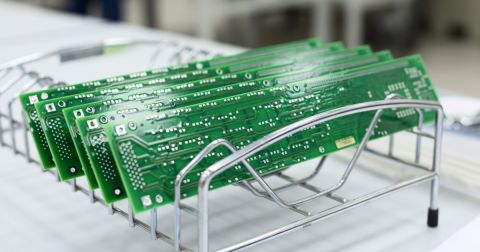
With the increasing complexity of multi-board designs, especially in applications such as automotive electronics, aerospace PCB systems, and IoT devices, effective board-to-board and harness integration has become more critical than ever. These connections form the backbone of reliable system-level performance, ensuring seamless communication between boards and robust interconnections.
Cable Harness Design: Proper cable harness design is essential for managing the interconnections between multiple PCBs. Engineers can reduce costly errors and ensure reliable, high-performance connections across complex multi-board PCB systems by planning and validating wire interconnections, connectors, and routing paths. This step is crucial for preventing signal interference and improper wiring that can lead to system failures.
Connector and Pin Mapping with Error Checking: Interconnect mapping is critical in large multi-board PCB systems, where pin assignments must be consistently defined and validated across different boards. This ensures the proper connections and reduces the risk of mismatches, minimizing the need for costly redesigns and improving overall system reliability.
Tracing connections through a PCB system from board to board can be one of the most tedious tasks, often feeling like chasing your tail. You trace the net, find an error, fix it, and then start again from the beginning. A good multi-board PCB design program can alleviate this frustration by helping you trace connections and automatically notify you of any errors as soon as they occur. You don't want to discover a dead-end route near the end of your design process—it's vital to identify potential issues from the start, saving you time and ensuring a more reliable final product.
Seamless MCAD and ECAD Collaboration and 3D Assembly
The improvements in integrating electronic (ECAD) and mechanical (MCAD) design tools have significantly transformed PCB design. This seamless ECAD-MCAD collaboration is crucial for multi-board PCB systems, which are increasingly complex mechanically. Engineers risk misalignment, clearance issues, and costly design iterations without proper integration when transitioning from PCB layout to mechanical assembly.
- Real-Time 3D Clearance Checking: Instead of waiting for mechanical engineers to validate fit, modern PCB tools now provide real-time clearance checking within the design environment.
- Component Height & Enclosure Fit Validation: Access to accurate 3D component models allows designers to check whether tall components like capacitors and connectors will fit inside enclosures before manufacturing.
Design Synchronization & Updates
Multi-board systems demand continuous synchronization between multiple PCB designs, ensuring that changes made to one board are accurately reflected across the PCB system. Design inconsistencies can lead to costly errors, misaligned interconnects, and functionality issues without proper synchronization. This becomes even more critical when dealing with complex board-to-board interconnections and cable harness designs, where a minor misalignment can cause system-wide failures.
- Automated Design Synchronization: Synchronization in multi-board projects is key to maintaining consistency across component placements, net assignments, interconnections, and cable harness configurations throughout the design process. System-wide updates to schematics, board layouts, or wiring harnesses can be made whenever changes occur. This prevents manual tracking errors and reduces the risk of design mismatches.
By integrating cable harness validation into the design synchronization process, engineers can ensure that all wiring interconnections are correctly mapped and updated across the PCB system. This eliminates misaligned connectors, incorrect pin assignments, and last-minute harness modifications, ensuring seamless communication and power distribution across all PCBs.
Beyond Multi-Board: Additional Capabilities That Enhance PCB System Design
While multi-board assembly is at the core of system-level PCB design, other capabilities further enhance the process:
- Interboard rule checking and enhanced EMI control
- Modular design, reusability, and easy redesign
- Rigid-flex and High-Density Interconnect (HDI) support
- Advanced manufacturing and Design for Manufacturing (DFM) tools
Interboard Electrical Rule Checking and EMI Control
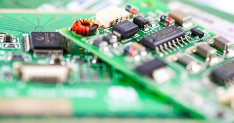
Interboard rule checking and enhanced EMI control are crucial for ensuring multi-board PCB designs' electrical integrity and performance. While checking electrical rules at the individual board level is straightforward, it becomes much more complex when dealing with multiple boards interconnected in a PCB system.
Advanced tools for inter-board rule checking allow designers to track connections across boards, ensuring that everything fits together electrically and mechanically. This capability is especially valuable when making design updates or adjustments during a redesign, such as when changes to an enclosure require significant modifications to interconnections.
Additionally, EMI reduction tools help to manage the routing of high-speed traces, differential pairs, and grounding while ensuring proper current return paths and signal isolation across boards.
FCC certification can be a hassle; you don't want to go through radiated or conducted emissions testing twice. There are many interference concerns when routing signals across boards, so you must be careful with analog and digital portions of your PCBs. Proper grounding is also essential, as you're probably unable to use a star ground.
These tools allow engineers to visualize and manage EMI risks, ensuring that their designs meet regulatory standards like FCC certification and preventing the need for repeated emissions testing. By providing greater control over these critical factors, these capabilities streamline the design process and minimize costly errors, ultimately ensuring system-level performance and reliability.
Modular Design, Reusability, and Easy Redesign
At first glance, modular design and reusability may not seem as thrilling as MCAD integration or system-level rule checking. However, they offer immense benefits in efficiency and flexibility. Modular design allows engineers to reuse components and subsystems from previous projects, reducing repetitive work and speeding up design iterations. Instead of reinventing the wheel, designers can incorporate proven components into new PCB systems, focusing on innovation rather than redoing what's already been done. This approach significantly reduces time wastage and boosts collaboration as different teams can work on separate modules simultaneously.
In addition, modular design makes redesigns easier. When system-level changes, like adjustments to enclosures, force alterations to the PCB design, manually tracking these modifications can become a nightmare. Tools that highlight nets and trace routing simplify this process, allowing designers to see the impact of changes visually and quickly make the necessary adjustments. By making the redesign process more streamlined and manageable, this feature reduces the risk of costly mistakes and ensures the overall integrity of the multi-board system.
Rigid-Flex and High-Density Interconnect (HDI) Support
Rigid-flex and High-Density Interconnect (HDI) designs are essential in modern electronics, particularly in industries such as automotive, aerospace, medical devices, and wearable technology. These design techniques enable engineers to create smaller, more efficient, durable PCB systems supporting complex functionalities.
Rigid-flex designs combine rigid and flexible PCB elements, allowing for greater design flexibility in tight spaces while maintaining mechanical strength. Best tools for rigid-flex designs streamline the process by supporting seamless transitions between rigid and flexible sections, automating layer stacking, and enabling precise clearance checking. Meanwhile, HDI capabilities allow for the creation of smaller and more compact designs through microvias, blind and buried vias, and optimized routing. HDI designs provide higher component density without sacrificing signal integrity, which is crucial for high-performance applications.
Modern tools support these advanced design techniques to ensure that engineers can meet the growing demands of miniaturized electronics while maintaining manufacturability and reliability.
Advanced Manufacturing and Design for Manufacturing (DFM) Tools
Design for Manufacturability (DFM) is a key consideration in the PCB design process, helping ensure that designs can be quickly and efficiently manufactured without introducing costly errors or delays.
Advanced DFM tools help identify potential manufacturing issues early in the design phase, allowing engineers to make informed decisions and optimize their designs for production. These tools perform real-time checks to ensure that the design meets the manufacturing capabilities of the PCB fabricator, such as verifying trace widths via sizes, component placement, and other critical parameters. They also support generating manufacturing documentation, including Gerber files and Bill of Materials (BOM), ensuring a smooth transition from design to production.
With robust DFM tools, engineers can avoid common manufacturing pitfalls, improve yield rates, and reduce time to market, making the design process more efficient and cost-effective.
Conclusion
Currently, only a few design programs combine all of the advanced features required for multi-board systems, and Altium stands out as a leader in this area.
Altium integrates an impressive set of tools that streamline and enhance the multi-board design process, making it easier to manage complex PCB systems and achieve seamless system interconnections. With its powerful features like real-time inter-board rule checking, 3D assembly visualization, and robust DFM tools, Altium simplifies multi-board design and manufacturing challenges. As Altium continues to push the boundaries of PCB design, its focus on rigid-flex, HDI, and modular design further enhances your ability to create innovative and efficient solutions. If you want to elevate your multi-board designs, Altium offers the ideal platform to bring your projects to life—accurately, efficiently, and error-free.
Interested in exploring multi-board PCB design? Discover how Altium Develop makes it easy to create complex designs and error-free system interconnections.

About Author
Related Resources
Related Technical Documentation
Table of Contents
- Multi-Board: The Core of System-Level PCB Design
- Board-to-Board Connectivity & Cable Harness Integration
- Seamless MCAD and ECAD Collaboration and 3D Assembly
- Design Synchronization & Updates
- Beyond Multi-Board: Additional Capabilities That Enhance PCB System Design
- Interboard Electrical Rule Checking and EMI Control
- Modular Design, Reusability, and Easy Redesign
- Rigid-Flex and High-Density Interconnect (HDI) Support
- Advanced Manufacturing and Design for Manufacturing (DFM) Tools
- Conclusion
Design to Release, Without the Friction
- Keep reviews tied to the right version
- Reduce handoff confusion and rework
- Spot sourcing and release risk earlier
- Work solo, share when needed
Get Started
Thank you, you are now subscribed to updates.

