


Multi-Board Design Adaptation in PCB Design Software

At a Glance
Adapt multi-board PCB design with modern software. Improve board-to-board connectivity, signal integrity & cable harness integration for complex systems.


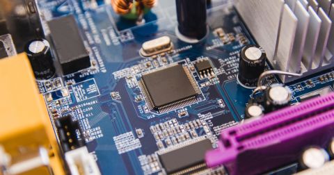
Innovation in electronics rarely stops at a single printed circuit board (PCB) design. Modern devices, from smart wearables and IoT hardware to autonomous automotive systems, rely on ecosystems of interconnected circuit boards. These boards must interact flawlessly, delivering both power and data across complex, compact architectures. That’s where multi-board PCB design finds its place as a cornerstone of system-level engineering
What Is Multi-board PCB Design?
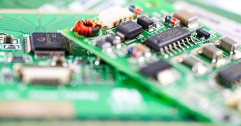
Multi-board PCB design structures electronic systems by distributing functionality across several specialized boards rather than crowding a single PCB. Each board tackles a specific function and connects to others via wiring or buses. These connections must deliver electrical performance while fitting within the mechanical confines of the final product.
Legacy workflows forced engineers to manage each PCB as an isolated design, making integration tedious and error-prone. Modern design platforms solve that disconnect, synchronizing multi-board systems from schematic to physical layout.
Why Multi-board PCB Adaptation Matters
To design a cohesive system, engineers must not only create individual boards but integrate them into a single, functional entity. Multi-board adaptation addresses the challenges that come with system-level complexity.
- Real-Time Collaboration: When teams split responsibility across multiple boards, collaboration becomes mission-critical. Today’s multi-board platforms provide a unified environment where updates sync instantly across designs. A change on one board propagates through the system, eliminating version mismatches.
- Simplified Interconnection Management: Routing signals and power between boards requires more than lines on a schematic. Engineers must account for signal integrity, impedance, and mechanical constraints. Modern tools map these interconnections with precision, validating them as part of the design flow.
- Maintaining Signal Integrity: Faulty signal paths introduce systemic errors. Advanced software detects impedance mismatches, crosstalk, and timing issues early. Built-in analysis ensures clean signal transmission across all boards.
- Mechanical Integration: Physical constraints affect electrical design. Boards must align correctly within enclosures, and interconnections (like cable harnesses) must match the spatial orientation of the device. Integrated 3D views offer real-time visualization to verify mechanical fit before production.
The Role of Cable Harnesses
In multi-board systems, cable harnesses manage power, signal, and data routing between PCBs, and thus these harnesses dictate both functional reliability and serviceability. Without them, even the most carefully designed multi-board PCBs wouldn't function as a cohesive unit. Here are just a few points why they play such a significant role:
- Reliable Connectivity: Cable harnesses ensure consistent signal and power delivery across the system.
- Signal Preservation: Engineered cable paths mitigate noise and minimize signal loss.
- Mechanical Fit: Proper harness layout prevents physical strain and reduces wear over time.
- Ease of Maintenance: Organized, labeled harnesses simplify diagnostics and repairs.
Modern PCB platforms now include features for simulating harness routing, verifying connector placement, and identifying space conflicts. These features guarantee that cable design aligns with the larger system from the outset.
What You Should Expect from Modern Multi-Board PCB Design Software
A comprehensive multi-board design platform goes beyond basic circuit creation. It integrates every phase of development into a single environment:
-
Board-to-Board Connectivity Tools: Engineers visualize interconnections and validate links with intelligent planning tools.
-
Integrated 3D Visualization: Teams inspect the full mechanical assembly, including cable harnesses and board enclosures, in real time.
-
Signal Integrity Analysis: Automated tools run simulations to verify the health of every signal path.
-
Design Rule Checks (DRCs): System-wide rules catch misalignments, voltage mismatches, and mechanical interference early in the process.
-
Collaborative and Version-Control Capabilities: Multiple stakeholders contribute to a single project space, with changes tracked across the system.
-
Cable Harness Integration: Design environments incorporate harness planning, ensuring every electrical and physical link functions correctly from day one.
Engineering for Tomorrow: Scaling with Innovation
As devices shrink and demand for high-performance functionality grows, multi-board PCB design faces increasing complexity. Upcoming advances—like flexible electronics and wireless interconnects—push traditional methods to their limits.
Fortunately, the software evolves just as quickly. Engineers continue to refine multi-board design platforms to meet next-generation challenges, helping teams build more compact, resilient, and highly integrated systems.
Aligning Systems from Concept to Completion
Mastering multi-board PCB design requires a system-level mindset that considers every component, from silicon to connector. Modern design tools empower engineers to unify electrical, mechanical, and manufacturing perspectives within a single design environment.
With synchronized workflows, in-depth validation tools, and robust cable harness support, today’s multi-board design software makes building complex systems more approachable, reliable, and scalable than ever before.
Interested in exploring multi-board PCB design? Discover how Altium Develop makes it easy to create complex designs and error-free system interconnections.

About Author
Related Resources
Related Technical Documentation
Table of Contents
Design to Release, Without the Friction
- Keep reviews tied to the right version
- Reduce handoff confusion and rework
- Spot sourcing and release risk earlier
- Work solo, share when needed
Get Started
Thank you, you are now subscribed to updates.

