Unveiling the Crucial Role of PCB Harness Design Capabilities in Interconnected Multi-Board Designs

The demands for innovation and efficiency continue to push the boundaries of technology. But as technology has evolved and products have demanded more complex features, the single-board designs of yesteryears are often no longer sufficient. Enter multi-board designs, which entail multiple PCBs interconnected to function as one unit. This sophistication, while powerful, demands a robust harness design for seamless and efficient interconnection. Here, we will delve into the importance of PCB harness design capabilities and how they are crucial for the success of interconnected multi-board designs.

The Essence of PCB Harness Design
Gone are the days when electronic devices were single, isolated entities. Today, devices are expected to communicate, share data, and seamlessly integrate with other systems. This paradigm shift has given rise to multi-board designs, where multiple PCBs are interconnected to form a cohesive electronic system, sharing electrical, mechanical, and functional connections. From consumer electronics to industrial applications, interconnected multi-board designs offer numerous advantages, including modularity, scalability, and improved reliability.
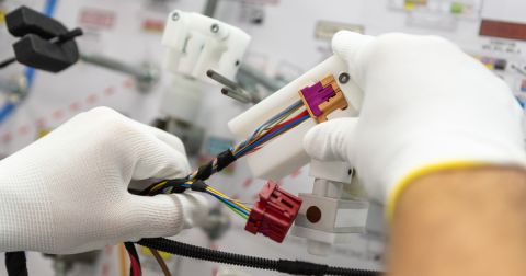
At the heart of every multi-board design lies the PCB harness – the intricate web of interconnections that enable the different boards to communicate and collaborate effectively. PCB harness design involves the thoughtful arrangement of connectors, cables, and signal traces to ensure optimal signal integrity, minimal electromagnetic interference (EMI), and efficient power distribution. The design process must take into account factors such as signal speed, impedance matching, thermal management, and electromagnetic compatibility (EMC).
Why Interconnected Multi-Board Designs?
Modern electronic products are getting smaller yet more powerful, and this presents a unique challenge. Integrating all required components onto a single PCB might not be feasible due to space constraints, signal interference, or thermal issues. This is where multi-board designs step in. By dividing a complex system into multiple interconnected PCBs, engineers can achieve several benefits:


-
Modularity: Interconnected multi-board designs allow for modular development, where each PCB can be designed, tested, and refined independently. Each PCB in a multi-board system can be designed and developed as a standalone unit. This allows engineers to focus on the specific functions and requirements of that board without being constrained by the complexities of the entire system. With modular designs, if a problem arises in one PCB, it can be identified and rectified without having to dissect the entire system. This segmentation simplifies the process of debugging and troubleshooting;
-
Performance Optimization: Multi-board systems allow for the design of PCBs that are tailor-made for specific tasks or functions. This ensures that each board is optimized for its primary role, be it signal processing, power management, or any other function. When each PCB is optimized for its specific role, the overall efficiency and performance of the entire system are boosted. This minimizes redundancies and ensures that each board performs at its best;
-
Easier Maintenance and Upgrades: In a multi-board design, if a single PCB malfunctions or becomes outdated, it can be replaced or upgraded without making changes to the rest of the system (e.g., WiFi module upgrade). This modular approach eliminates the need to overhaul or replace the entire system, saving time and costs. As technology evolves, specific parts of a system might need updates. With an interconnected multi-board design, these updates become more manageable and affordable as only the necessary PCBs need to be altered or replaced;
-
Heat Dissipation: In a multi-board system, components that generate significant heat can be strategically placed on separate boards. This segmentation allows for more effective heat management and distribution. By isolating heat-producing components on individual PCBs, there's a reduced risk of one component's heat adversely affecting another's performance. This layout can improve the longevity and reliability of the system by reducing potential overheating problems.
The Crucial Role of PCB Harness Design Capabilities
Harnessing the power of advanced PCB harness design capabilities becomes essential when dealing with multi-board designs. Here's why:
-
Signal Integrity: In interconnected multi-board systems that have grown in complexity, the preservation of signal integrity is pivotal to prevent system malfunctions or total failures caused by distorted or lost signals. ECAD tools with advanced harness design capabilities that also include advanced impedance control functions equip engineers with the necessary tools to safeguard this integrity throughout the multi-board, enabling them to optimize trace routing and thus reduce potential signal interference. These tools are also instrumental in mitigating issues like crosstalk, where signals from distinct traces might conflict, by facilitating the spatial separation of traces and the design of effective shielding;

-
Power Distribution: In interconnected multi-board systems, the consistent and reliable distribution of power across all interconnected PCBs is paramount for optimal functionality. Harness design capabilities empower engineers to craft precise power planes and routes, ensuring every PCB gets the necessary voltage/current. This strategic approach curtails power-related challenges such as drops or surges, safeguarding the overall system's performance;
-
Mechanical Integration: In multi-board setups, fitting several PCBs into one device enclosure requires careful planning to avoid physical interference. Beyond just electrical aspects, ECAD tools with harness design capabilities that also include true 3D modeling capabilities allow engineers to preview and visualize the system's physical configuration and layout, helping to spot and address potential collisions between components and ensuring proper PCBs fit, form, and function;
-
Cross-Board Communication: For multi-board systems to operate harmoniously, effective inter-PCB communication is crucial. Harness design tools are central to this, aiding in the development of high-speed interfaces, connectors, and bus architectures for swift and dependable data transfer between boards. Further, ECAD tools that also include a precise connection management function enable designers to easily define, modify, check, and update multi-board connectivity as the overall product design is developed.
The Future of Harness Design in Interconnected Multi-Board Systems
Multi-board designs have become the norm rather than the exception. Achieving successful multi-board integration requires a deep understanding of PCB harness design capabilities. A well-designed harness ensures signal integrity, modularity, scalability, reduced EMI/EMC issues, efficient thermal management, and overall system reliability. As the complexity of electronic systems continues to grow, the importance of mastering PCB harness design for multi-board designs cannot be understated. With the right tools, expertise, and attention to detail, engineers can pave the way for the next generation of interconnected and high-performing electronic devices.
Want to seamlessly design wiring for your harness? Experience the power of wire harness design in Altium Develop.
