


Eliminate EMI and Signal Integrity Issues in Multi-Board PCB Designs

At a Glance
Tackle EMI and signal integrity issues in multi-board PCB systems with proven strategies for grounding, layout, interconnects, power, and thermal design.


Modern electronics increasingly depend on multi-board PCB systems to deliver the performance, modularity, and scalability demanded by cutting-edge applications. From aerospace systems to advanced computing clusters, these designs push technological boundaries, but they also introduce complex challenges. Among the most critical issues are electromagnetic interference (EMI) and signal integrity (SI). Poorly managed interconnects, inconsistent grounding or inadequate shielding can lead to signal degradation, system instability, and even regulatory failures.
This article explores practical strategies to tackle these challenges, focusing on how engineers can optimize layout design, grounding, interconnects, power delivery, and thermal management to build reliable interconnected multi-board systems.
Multi-board designs are more than just interconnected PCBs. They’re ecosystems where electrical, thermal, and mechanical factors collide. Unlike single-board designs, interconnected multi-board systems rely on connectors, cables, or flex circuits to pass signals between boards. These transitions create potential weak points: impedance mismatches at connectors can reflect signals, long stubs in traces can resonate like tuning forks, and inconsistent grounding can turn return paths into antennas for noise.
For instance, a high-speed signal traveling from a processor board to a memory module might encounter a connector with a mismatched impedance. This discontinuity can cause reflections, distorting the signal and leading to timing errors. Similarly, heat from a power board stacked beneath a sensitive analog board can alter component behavior, subtly degrading performance. Addressing these issues requires a holistic approach that balances electrical precision with mechanical pragmatism.
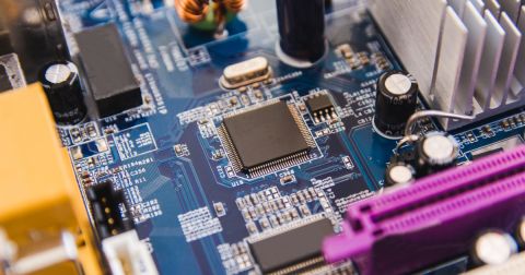
Laying the Foundation: PCB Layout and Routing
The journey to a robust PCB multi-board system begins with a thoughtful PCB layout. High-speed signals demand meticulous routing to avoid distortion and noise. One fundamental rule is maintaining controlled impedance across traces, connectors, and cables. This means selecting trace widths and dielectric materials that match the interconnected multiboard system’s target impedance, typically 50 or 100 ohms. For example, a 10 Gbps serial link on a server backplane requires precise trace geometry to prevent signal loss.
When routing, prioritize high-speed signals by giving them a clear path over continuous ground planes. These planes act as shields, containing electromagnetic fields and providing stable return paths. Avoid running sensitive traces parallel to noisy power lines, as inductive coupling can inject noise. Instead, route them perpendicularly to minimize interaction.
Crosstalk is another silent saboteur. Increasing the spacing between high-speed traces reduces capacitive and inductive coupling. For differential pairs, tightly coupled routing ensures noise cancels out while avoiding right-angle bends prevents impedance spikes. Imagine a pair of high-speed USB traces: a sudden 90-degree turn could create reflections, much like a car swerving abruptly on a highway.
Grounding: The Key to EMC and Signal Integrity
Grounding is often treated as an afterthought, but in PCB multi-board systems, it’s the backbone of EMC and SI. A fragmented ground strategy can lead to ground loops, where voltage differences between boards create circulating currents that radiate noise. To prevent this, establish a single, unified ground reference across all boards. In the case where certain boards contain signal isolators or isolated DC/DC converters, create clear delineations between different ground regions. Where applicable for suppression of high-frequency radiated emissions, use a Y-type safety capacitor to connect grounds while maintaining DC galvanic isolation and ESD protection.
To see an example of how to properly do this, watch the following video:
Continuous ground planes in each region are equally vital. They minimize impedance variations and act as electromagnetic shields. When stacking boards, insert a ground plane between layers to isolate noise. For example, in a stacked IoT sensor module, a ground plane between the RF and digital layers can prevent radio interference from corrupting sensor data.
Ground stitching vias—small plated holes connecting ground layers—are another powerful tool. Placing them strategically around high-speed connectors or noisy components ensures low-impedance return paths. Picture these vias as bridges that keep the ground network cohesive, even across complex layouts.
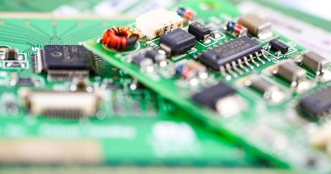
Interconnects: Bridging Boards Without Compromise
Connectors and cables are the lifelines of interconnected multi-board systems, but they’re also prime suspects for EMI and SI issues. Choosing the right signal integrity connectors is akin to selecting a bridge design: it must handle the traffic (signal speed) without collapsing (introducing losses). Opt for impedance-controlled connectors that match your PCB’s trace impedance. For instance, a high-speed PCIe connector with matched impedance ensures seamless signal transitions between boards.
Stub lengths—those unintended branches in connectors or traces—are another pitfall. Like an echo in a hallway, stubs can cause resonant reflections. Keep signal paths as direct as possible, and avoid unnecessary splits. When routing through connectors, ensure signals transition cleanly without meandering.
Cable selection also matters. Twisted-pair or coaxial cables excel at rejecting noise, while shielded variants add an extra layer of defense. For critical signals, such as clock lines in a medical imaging system, shielded cables act as armor against external interference.
Power Delivery: Keeping the Lights On Without the Noise
A stable power supply is the lifeblood of any electronic system, but in multi-board designs, noise from one board can ripple through others. Decoupling capacitors are the first line of defense. Placing them near IC power pins is like stationing firefighters next to a hazard—they can instantly suppress voltage spikes. Combine bulk capacitors for low-frequency noise and smaller ones for high-frequency ripples.
A well-designed power distribution network (PDN) helps reduce EMI. Wide power traces minimize resistance and voltage drops, while ferrite cores on power lines filter out high-frequency noise. Conducted EMI can be further suppressed by incorporating common-mode chokes and low-pass filters, preventing unwanted signals from interfering with system operation. Proper grounding of power planes is also crucial. Multiple power planes must connect to a common ground reference to prevent noise from propagating between different voltage domains.
Thermal Management: Cooling Without Compromise
Heat is the silent enemy of signal integrity. As temperatures rise, materials expand, altering trace impedance and component behavior. In a multi-board setup, heat from one board can cascade onto others. Thermal vias—small holes filled with conductive material—act as highways for heat, channeling it away from hotspots. For example, in a GPU cluster, thermal vias under the processor transfer heat to a metal core, which a heatsink then dissipates.
Active cooling, like fans or liquid systems, is essential for high-power applications. However, airflow must be optimized to avoid cooling one component while overheating another. Strategic placement of vents and ducts, guided by 3D thermal simulations, ensures even cooling.
Material choices also play a role. Metal-core PCBs or substrates with high thermal conductivity, such as aluminum nitride, can turn the board itself into a heatsink. In an automotive control unit, these materials prevent heat from warping nearby traces, preserving signal fidelity.
Mechanical Integration: Where Form Meets Function
A PCB multi-board system’s mechanical design is as crucial as its electrical blueprint. Cables and harnesses must be routed to minimize inductance and crosstalk. Keeping power and signal cables separate avoids noise coupling. Think of them as rival siblings who need their own space.
ECAD tools with true 3D modeling and advanced MCAD integration, like Altium, allow engineers to visualize how boards and cables fit together before fabrication. This prevents last-minute surprises, such as a connector colliding with a heatsink. Strain relief mechanisms, like cable clamps or flexible PCB sections, protect connections from mechanical stress, ensuring longevity.

Conclusion: Building Resilience Into Multi-Board Systems
Designing multi-board PCB systems requires a comprehensive approach that integrates PCB layout best practices, grounding strategies, optimized interconnects, effective power distribution, and thermal management. Engineers must proactively address EMI and signal integrity challenges by leveraging modern tools and following industry best practices.
With the increasing complexity of electronic systems, robust PCB harness design and EMI control are no longer optional. They are essential for ensuring reliability, compliance, and performance in next-generation multi-board PCB designs.
Interested in exploring multi-board PCB design? Discover how Altium Develop makes it easy to create complex designs and error-free system interconnections.
About Author
Related Resources
Related Technical Documentation
Table of Contents
- The Hidden Complexities of PCB Multi-Board Systems
- Laying the Foundation: PCB Layout and Routing
- Grounding: The Key to EMC and Signal Integrity
- Interconnects: Bridging Boards Without Compromise
- Power Delivery: Keeping the Lights On Without the Noise
- Thermal Management: Cooling Without Compromise
- Mechanical Integration: Where Form Meets Function
- Conclusion: Building Resilience Into Multi-Board Systems
Design to Release, Without the Friction
- Keep reviews tied to the right version
- Reduce handoff confusion and rework
- Spot sourcing and release risk earlier
- Work solo, share when needed
Get Started
Thank you, you are now subscribed to updates.