


Types of Simulation Tools For PCBs

At a Glance
See the types of simulation tools for PCBs in this article. There is no single simulation feature designers can use. Instead, there are many types of simulation software.


There is no single simulation application or analysis approach for PCBs. The goal in simulation software is to model specific physical processes, whether they are mechanical, electrical, or thermal. The simulation software available today for general purpose use can also be used for PCBs, giving designers and teams many options for simulation and board qualification.
This article will give a list of the simulation options available for PCBs. These include commercial software, open-source packages, and features integrated into your PCB design application.
Commercial PCB Simulation Software
The best-known simulation tools for PCB designers are commercial software packages. These packages provide electrical, mechanical, thermal, or multiphysics capabilities in complex geometries. Some software packages are highly specialized for PCBs and electronic products, tending to focus on specific types of simulations in PCBs. Commercial software options for
Ansys
Ansys offers a comprehensive suite of simulation tools to analyze electrical, thermal, mechanical, and multiphysics aspects of printed circuit boards (PCBs) and electronic systems. For designers, specialized products address core areas of analysis.
These tools are often combined in multiphysics workflows, allowing for coupled analysis, such as linking electrical losses to thermal rise and mechanical stress.
- HFSS and SIwave: Used for 3D electromagnetic simulation, covering signal integrity, power integrity, EMI/EMC, and antenna behavior.
- Icepak: Supports detailed thermal analysis for boards, packages, and enclosures, including airflow and conjugate heat transfer.
- Structural solvers: Enable mechanical stress, vibration, and reliability simulations, addressing issues like warpage, solder joint fatigue, and enclosure interactions.

[Source: Ansys]
Keysight ADS
Keysight ADS is a comprehensive tool for RF, microwave, and high-speed digital design, offering schematic simulation, harmonic balance for nonlinear RF, EM field solvers, and channel simulation. It supports co-simulation to integrate S-parameters from PCB structures into system-level simulations. ADS is essential for validating impedance, matching networks, filter responses, and channel compliance in RF PCBs and high-speed interconnects.
Simbeor
Produced by Simberian, the Simbeor simulation software package is highly optimized for PCBs and package substrates, specifically focusing on signal integrity and channel verification. Pre-layout simulations can be performed to validate stackups, vias, and transmission line geometry, while post-layout simulations provide a highly accurate view of signal integrity in the PCB layout. Automated channel compliance tools and a new agentic workflow help users set up projects and quickly validate designs against standard computing interfaces.

[Source: Simberian]
COMSOL Multiphysics
COMSOL Multiphysics provides a flexible environment for coupled thermal, electrical, structural, and electromagnetic simulations. For PCBs, it can be used to model complex multiphysics interactions, where the interplay between multiple physical phenomena needs to be understood. Some of the possible computational capabilities include:
- Joule heating in copper traces in DC and AC
- temperature distribution across multilayer boards
- mechanical stress due to CTE mismatch
- low-frequency electromagnetic effects
Because it is not PCB-specific, users build models from geometry upward, which provides flexibility at the expense of additional setup effort. COMSOL is often selected when custom physics coupling or nonstandard materials must be analyzed, which often confines it to specialized research topics or academic settings.
Open-Source PCB Simulation Software
Open-source simulation tools are also available for PCB-related analysis. While they generally require more manual setup and may lack specialized PCB automation features, they can provide credible electrical, thermal, and mechanical modeling capabilities for teams willing to invest the time in configuration and validation. Common options include:
- OpenEMS: A 3D electromagnetic field solver used for post-layout signal integrity, RF design, EMI/EMC investigations, antenna analysis, and transmission line modeling.
- ngspice: Circuit-level simulation for analog, mixed-signal, and behavioral modeling.
- FreeCAD (with FEM workbenches): Mechanical modeling and structural simulations for enclosures and board supports.
- QUCS: A schematic-based circuit simulator supporting DC, AC, transient responses, S-parameters, and RF circuits.
- Elmer FEM: Multiphysics solver capable of thermal, structural, and electromagnetic analysis.
- OpenFOAM: Computational fluid dynamics for airflow and cooling simulations in enclosures containing PCBs.
Open-source simulation software offers an obvious cost advantage, particularly for small companies and students. However, it typically requires greater expertise in meshing, solver configuration, scripting, and validation against reference data. PCB-specific automation, compliance templates, and integrated material libraries are generally less developed compared to commercial platforms.
Integrated Simulation in PCB Design Software
Although there are many simulation options for PCBs, systems, and electronic components, most of these are available as external applications requiring their own licenses. The simulation capabilities inside PCB software tend to be quite limited, but fortunately some PCB design platforms provide a few important capabilities which are included as standard features.
SPICE Simulation
Some PCB design platforms include SPICE simulation directly from the schematic environment. Examples include Altium Designer and Cadence OrCAD with PSpice integration. These tools allow designers to simulate analog and mixed-signal circuits before layout. Among mainstream PCB platforms, Altium supports multiple SPICE model formats, including LTSpice and PSpice models, enabling designers to reuse vendor-provided component models without extensive reformatting.

SPICE within PCB design software is typically used for mixed-signal simulation, covering analog circuits, equivalent behavioral models of digital components, switching regulators, and certain ASIC models. Designers can create custom components, assign proprietary or encrypted models, and integrate these models into hierarchical schematics for system-level validation prior to layout.
IBIS Simulation
IBIS (Input/Output Buffer Information Specification) simulation uses standardized behavioral models to represent the electrical characteristics of device I/O pins. Higher-end PCB design tools and external SI applications support loading IBIS models and assigning them to specific pins in a design. These pin models are then used to define stimulus and termination behavior in signal integrity simulations.
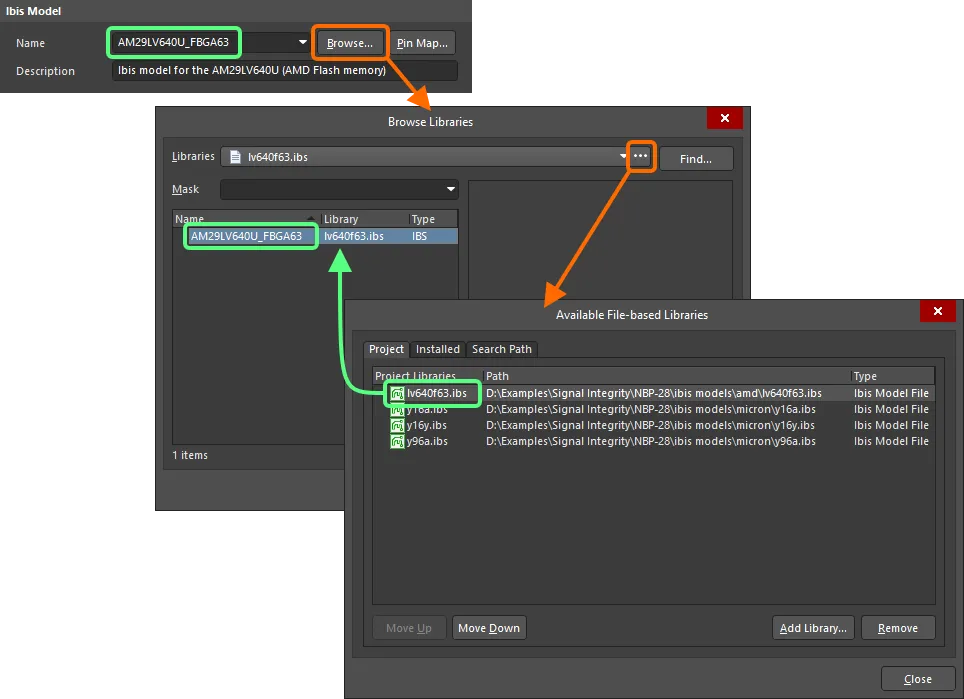
How to add IBIS models to pins in Altium Designer
We use IBIS models on specific pins to more accurately capture how a device driver or receiver sources/sinks a signal. Instead of assuming an ideal voltage source, the IBIS model accounts for edge rates, output impedance, and voltage-current characteristics. This is particularly useful for modeling high-speed digital signals without knowing all the internal details of the device package, die circuitry, etc.
Post-Layout Reflection and Crosstalk Simulation
Higher-end PCB design platforms also include post-layout signal integrity tools that evaluate reflection and crosstalk directly from the routed PCB. These tools may use generic logic family definitions or IBIS models for pin behavior and apply numerical techniques such as boundary element method (BEM) or method of moments (MoM) solvers.

The results provide a fast evaluation of signal integrity on selected nets without manually building a mesh or testing against reference data. There is no need to export to an external program or setup complex configuration other than pin/stimulus definitions.
Impedance Calculations in the PCB Layout
Most PCB layout tools do not include full-field impedance solvers as a standard feature, even though impedance control is mandatory for many high-speed interfaces. Some platforms integrate field-solving capability directly into the stackup editor. For example, Altium Designer includes Simbeor’s cross-sectional field solver in the Layer Stack Manager, allowing users to calculate lossless impedance values without exporting to an external application. This capability enables designers to determine trace geometries and define these as design rules on selected nets before starting the PCB layout.
Signal Analyzer and Power Analyzer by Keysight
Altium Designer offers an integrated solution for signal integrity calculations directly from the PCB layout with the Signal Analyzer tool from Keysight. There is also a tool for DC power integrity, which is the Power Analyzer tool that also runs inside the PCB layout. Both features bring a level of visualization to an entire interconnect which normally requires a full-wave electromagnetic simulator, but can now be accessed inside Altium Designer.

Which Simulator Should You Use?
The appropriate simulator depends on what physical behavior you need to evaluate. Circuit-level behavior can often be addressed with SPICE. High-speed interconnects may require IBIS-based channel simulation or 3D EM analysis. Thermal management might demand CFD or multiphysics tools. In many workflows, PCB designers combine integrated schematic simulation, impedance calculation in the stackup, and targeted post-layout SI checks, then escalate to specialized commercial tools for final verification or compliance work.
Whether you need to build reliable power electronics or advanced digital systems, use Altium’s complete set of PCB design features and world-class CAD tools. Altium provides the world’s premier electronic product development platform, complete with the industry’s best PCB design tools and cross-disciplinary collaboration features for advanced design teams. Contact an expert at Altium today!
Frequently Asked Questions
What is the best simulation tool for PCBs?
There is no single “best” tool. The correct choice depends on whether you are analyzing circuits, signal integrity, thermal performance, EMI/EMC, or mechanical stress.
Can I simulate a PCB directly from my layout software?
Some PCB design tools include post-layout signal integrity checks and impedance calculators, but full 3D electromagnetic or multiphysics simulation usually requires external software.
Is SPICE enough for PCB simulation?
SPICE is useful for circuit-level validation but does not model 3D electromagnetic coupling, radiation, or detailed thermal behavior of a PCB.
What is IBIS simulation used for?
IBIS models represent real device I/O behavior and are used to simulate high-speed digital signals, reflections, and timing margins on PCB interconnects.
Are open-source PCB simulators reliable?
They can be reliable when properly configured and validated, but they generally require more manual setup and domain expertise than commercial PCB-focused tools.
Do I need 3D electromagnetic simulation for every PCB?
No. 3D EM simulation is typically reserved for high-speed digital channels, RF circuits, antennas, or EMI/EMC troubleshooting where distributed effects dominate behavior.
About Author
Related Resources
Related Technical Documentation
Table of Contents
- Commercial PCB Simulation Software
- Ansys
- Keysight ADS
- Simbeor
- COMSOL Multiphysics
- Open-Source PCB Simulation Software
- Integrated Simulation in PCB Design Software
- SPICE Simulation
- IBIS Simulation
- Post-Layout Reflection and Crosstalk Simulation
- Impedance Calculations in the PCB Layout
- Signal Analyzer and Power Analyzer by Keysight
- Which Simulator Should You Use?
- Frequently Asked Questions
Design to Release, Without the Friction
- Keep reviews tied to the right version
- Reduce handoff confusion and rework
- Spot sourcing and release risk earlier
- Work solo, share when needed
Get Started
Thank you, you are now subscribed to updates.

