


Vias 101. What Is a PCB Via?

At a Glance
In this blog, Phil Salmony offers beginner PCB design engineers a good starting point to understanding vias. We will tackle the basics and recommended parameters. Read now to learn more.


In this “Vias 101” article, we will be covering the very basics of vias in PCB design, including their characteristic parameters, which standard vias should be used in designs, and talk briefly about current handling capabilities. We will also examine proper placement of vias, and special use cases such as transfer and stitching vias.
Keep in mind that there are far more parameters and details to vias in PCB design then we will be able to cover in this short article. However, the article will provide beginner PCB design engineers with a good starting point to be able to delve deeper into the topic. Let’s get started!
Vias: Basics
Let's start off with via basics. We know that traces are connections on a single X-Y plane, starting from one point on a layer and ending at a different point on the same layer. However, once we want to route between layers, for example connecting layer one to layer three in a multi-layer PCB, we need to use something called a via. Essentially, a via is a conductive, vertical connection in the third (Z) dimension, and is used for connections between layers, allowing a trace on one layer to jump to any (or multiple) layers in a PCB.
Another way of thinking about a via is considering it to be a miniature plated through-hole.
Keep in mind that if we're not connecting to a certain layer with a via, we will create a void on that layer. This can cause problems, as we will see later. The image below shows a void, where we have an anti-pad in the layer we are passing through.
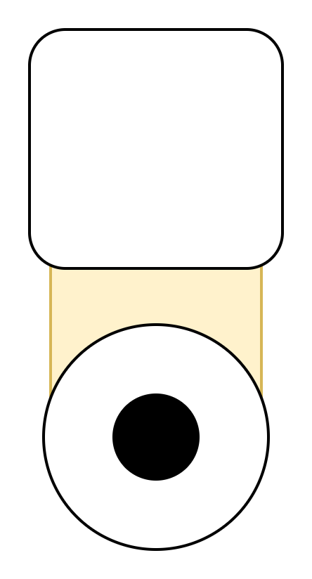
Vias: Sizing Parameters
When talking about vias, we have certain main parameters that define them. The image below shows a typical through- via, defined by the pad size P (the overall via diameter), and a drill size D.
The drill size must always be smaller than the pad size, and is limited by the aspect ratio (the ratio of PCB thickness to drill size). This is a manufacturing problem, and depends on your board thickness. - The thicker your board is, in general, the larger drill size you need.
Furthermore, if we subtract the drill diameter D from our pad size P, and divide that number by two, we get the size of the annular ring. Both the drill size and the annular ring size are important manufacturing parameters.
Typically, without adding cost, the minimum drill size is 0.25 mm and the minimum annular ring is 0.15 mm. However, it is important that we stay away from minimums if we can’t otherwise avoid doing so. When it comes to PCB manufacturers, many will offer more advanced capabilities, for example 0.1 mm drills (usually lasers). Keep in mind that this adds costs.
When sizing your vias, other than drill sizes, pad sizes, and annular rings, there are many other parameters that make up a via. For example:
- Tenting: Covering the via with a solder mask. Typically no extra cost.
- Filling: Filling with resin or conductive material, which can be useful for via-in-pad technology. This will be an extra cost.
- Type: In this article, we are looking at through-vias (the easiest to produce and most common). However, there are other types such as micro, blind, and buried, to name a few. These are topics for future articles.
Via Sizing: Recommended Parameters
It is difficult to give general recommendations for via parameters. The parameters you ultimately should use in your design depends strongly on the scenario. For example, if you’re routing out a very fine-pitch BGA, your via needs will be completely different to routing out an audio through-hole-only component board.
In terms of cost, a small drill size (usually anything less than 0.2 mm) will typically give an increased PCB manufacturing cost and a lower yield. Yield meaning that maybe 90% of the PCBs manufactured will work, and 10%will be defective.
The same thing goes for a small angular ring (around 0.1 mm). Again, the PCB manufacturing cost will increase and the yield will decrease.
“What size of via should I use?” I get this a question a lot‘’), and as a general purpose via I can recommend the following sizes:
- Large: 0.7 mm pad, 0.3 mm drill
- Medium: 0.6 mm pad, 0.25 mm drill
- Small: 0.5 mm pad, 0.2 mm
Again, this is a general guideline, and the actual via dimensions will depend on the given scenario.
Via Standards: Current Handling Capabilities
When we are discussing vias, we also need to think—as with traces—about the current handling capabilities. Traces can handle a certain amount of current for a given temperature rise, and vias are no different.
As a rule of thumb, a typical ”‘standard-sized” via can sustain about 1.5 A for a 20 degree Celsius temperature rise. If you require more than that current, for example in an ESC’s motor drivers, we simply need to use parallel vias of the same size. In contrast, for traces we simply have to widen the trace. However increasing the drill and pad sizes for a via only marginally increases the current handling capabilities but paralleling vias aids in reducing inductance and improves thermal performance.
Via Spacing and Sizing Standards: Placement
Regardless of if we are dealing with traces, components, outlines, vias, and so on, we always need to think about clearances between these elements, such as between vias and traces, vias and vias, vias and pads, and so on. As usual, minimum clearances are detailed by your chosen PCB manufacturer or standard. However, I would advise you to stay away from these minimums, not only for manufacturing reasons but also for other reasons such as cross-talk.
Additionally, when we are looking at power and ground vias, we want their connections to relevant component pads to be as short and as wide as possible to minimise inductances. This doesn’t mean placing the vias in or directly adjacent to any pad but a reasonable distance away so that you don’t get problems with solder wicking.
As vias come in pairs, we want to typically place power and ground vias close together to minimise inductance, and improve power delivery characteristics.
Via Spacing: Voiding
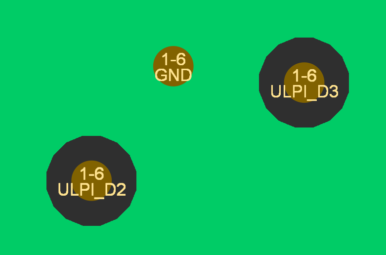
When spacing vias closely to one-another we get an issue known as voiding. Essentially, for through via (vias that go through the whole thickness of the PCB), placing vias close to each other can cause cuts in the reference plane due to the via anti-pads being too close together. An example of this can be seen below in the image of a GND plane with too-closely spaced non-grounded vias. This will impede return currents, and can potentially cause EMI problems.
The problem of voids in dense designs can be hard to avoid, especially when you have a large number of signal vias in a particular area. Again, if we were to route a trace over the split in the reference plane caused by voiding, it can be very harmful to EMI performance. The return currents will have to flow around this split in the reference, causing fields to spread, and will increase the radiation and EM signature.
If space allows, a simple fix to mitigate voids in reference planes is to place vias far enough apart from each other so that copper can flow in-between these via anti-pads.
An alternative method is to use HDI vias, either micro-vias to decrease the size of the anti-pads, or blind and buried vias that do not penetrate reference planes. However, this is of course bound to an increase in PCB manufacturing cost.
In any case, make sure to always check your reference planes during the stage of layout and routing for voids. I highly recommend scanning your final Gerber output files for voids as well.
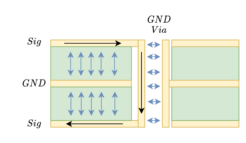
Transfer Vias
When switching layers with a signal via, we typically also change reference planes (think of a four-layer SIG-GND-GND-SIG board, for example). While we’re still routing on the top layer with a trace, for AC signals (>20 kHz), the return path is directly in the reference plane below. Once we are on the bottom layer, the return path is in the reference plane above.
What happens to the return path and thus the fields when we move along the via in the Z-axis when changing layers? Then fields will spread as they try to find a suitable “attachment point” (a return path), which in turn can be a cause of EMI problems. In such cases, we want to place a transfer via— which is basically a grounded via— close to the signal via. This is to maintain a defined reference and return path while transitioning along the Z. Note that this transfer via only works if the references we are switching between are both of the same type (for example, GND to GND).
If we’re switching from a GND to PWR reference, we need to place a small-valued capacitor stitched between GND and PWR reference close to the transition point.
Stitching Vias
There are two main reasons for stitching vias. Often in single, multi-layer PCB designs we have multiple ground or power layers, and multiple ground or power copper pours. Without stitching vias (either ground or power vias), the various ground and power layers, as well as any other ground or power copper pours, wouldn't connect well together. A voltage difference would be created between them, in particular at higher frequencies due to impedance, and specifically inductance. To mitigate this, we need to tie these together with vias.
By placing stitching vias, we can tie these layers and pours together at several X-Y locations on the PCB.. Additionally, every time we have copper islands, which can often be not attached at all (or poorly attached) with just a small number of vias, these copper islands can act as antennae, resonate, and then even radiate. This can of course be very harmful to a board’s EMI performance.
The second reason or use for stitching vias is for shielding purposes. In effect, we can use a “wall” of shielding vias to suppress energy of electromagnetic waves (up to a certain frequency) from entering or leaving a section of the PCB. The spacing of shieldings is determined by the maximum frequency apparent in a PCB. For example, for an audio PCB this frequency might be 20 kHz, and for an RF PCB it could be 2.4GHz, if not even higher.
Once you know your maximum frequency of your PCB, we simply need to use this formula to calculate the spacing, where c is the speed of light, ε is the dielectric constant, and f our maximum frequency of interest:

For example, at 2.4 GHz, and with routing on outer-layer (microstrip) traces, the formula gives us a stitching via spacing of 3.4 mm.
Via Sizing, Spacing, and Standards
In this article, we have examined the basics of vias in PCB design, looking at via parameters, such as drill and pad sizes, types of vias, and what vias can be used for, including transfer and stitching vias.
Make sure to check out all of Altium’s built-in via features, including capabilities for handling more complicated types of vias found on HDI boards, such as micro-vias, blind, and buried.

About Author
Related Resources
Related Technical Documentation
Table of Contents
Design to Release, Without the Friction
- Keep reviews tied to the right version
- Reduce handoff confusion and rework
- Spot sourcing and release risk earlier
- Work solo, share when needed
Get Started
Thank you, you are now subscribed to updates.