


Part 1: Setting Up Your Fabrication Document

At a Glance
Learn everything you need to know about Documentation for Fabrication and Assembly of printed circuit boards.


Before you can send your design off to manufacturing, you will need to ensure that it is properly documented to clearly communicate your design intent. While electronic files such as Gerber and ODB++ provide enough basic information to make your board, they don’t include all of the fine details from your head about how you intend to have your board produced.
The documentation stage is your chance to precisely describe your board layout and avoid any design intent miscommunications that typically occur when design goals are not clearly conveyed. This portion of our guide series will focus on creating a standard PCB documentation template and outlines all of the necessary details you will want to include to increase understanding by your manufacturer. The next chapter will then go into the specifics of your master drawing. If you would like to skip ahead to different chapters in this series, use the Table of Contents links below:
- Setting Up Your Fabrication Document
- Documenting Your Master Drawing
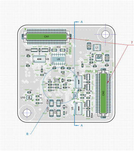
- Documenting Your PCB for Assembly
- Creating Fabrication and Assembly Drawings In Altium Designer
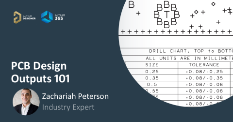
Drawing Sizes
The first step in creating a master drawing is selecting an appropriate drawing area to contain all of your drawings. The dimensions of your drawing area are referred to as the drawing size and should comply with the ANSI-Y 14.1[6-1] standard sizes as shown below. If possible drawing sizes should be kept consistent for all documentation while still adhering to your company's documentation policies.

Once the drawing size is selected, there are several blocks that need to be included in the PCB drawing. A block includes additional details and specifications that will help to clearly define your design requirements for manufacturing and should be fully detailed to avoid any potential production delays or errors.
Zoning
Zoning is used to provide reference to a drawing and is especially useful with multi-sheet drawings. Although you can zone a drawing in several ways, it is recommended to choose one method and use it throughout all of your designs for the sake of consistency. We'll implement the following guidelines as we continue in this tutorial:
- The horizontal borders (top and bottom) of the drawing sheet need to be labeled starting with “A” at the top leftmost part of the drawing and increasing alphabetically as you move to the right.
- On the vertical sides (left and right) start with “1” on top and continue downward while increasing numerically as you move down.
- All letters should be capitalized.

Title and Revision Blocks
The Title Block is an important part of your PCB drawing as it communicates to your manufacturer basic information necessary for manufacturing your board. When creating the Title Block, there are many different sections you will need to provide, including:
- Drawing title and subtitle
- Drawing scale
- Drawing number
- Approval block

The figures below show these sections on the title block in more detail with some additional information.
Title Area
Place a descriptive title in the title block so your collaborators, customers, and manufacturer can keep track of the document and the PCB.

Scale
The Scale is ratio of the actual design to the image and should be described in fractional form.

Drawing Number (DWG. NO.)
A drawing number will help everyone involved in a project keep track of documentation. Some documents may include a part number or revision number built into the drawing number.

Cage Code (if applicable)
The Cage Code is a five-character string used by the U.S. federal government to identify a business establishment. This is normally not needed in fabrication drawings that do not deal with government or military PCBAs.

Approval Block
The Approval Block is used to for individuals (drafters, designer, checker, etc.) to sign off on a design. This block is designed to cover approvals at multiple stages in the design and production process.

Although requirements can be different depending on your organization’s established CAD standards, the five sections above are considered to be the minimum requirements needed for a title block. You should work to establish your own title block standards for future projects. The blocks shown in the figures below include optional details that might be relevant to your project’s specifications.
Application Block
The Application Block is optional and segmented into two parts, the first being the ‘USED ON’ section and the other being the ‘NEXT ASSY’ section. The ‘NEXT ASSY’ section tells the engineer the next assembly the part will be used in, while the ‘USED ON’ refers to the main assembly that houses the next assembly.

Revision Block
The Revision Block is used to keep track of the project revision and can be seen in Figure 62 below. Make sure to adhere to your company's revision scheme, but if no scheme is in place use the suggested revision scheme below:
- The first revision is shown as an “A”
- The second revision is shown as a “B” and so on
- If you run out of letters introduce a second letter. “AA” → “AB”

Contract Number
If the drawing is specified in a certain contract or other document, then the Contract Number block is the place to put this information. This could also be used to place a purchase order number.

Distribution Key
The Distribution Key is used for in-house distribution to certain departments in your organization and should be placed directly above the Title Block.

Material Block
The Material Block contains numbers corresponding to the appropriate notes that are included elsewhere in the drawing. Specifically, these notes should state the materials being used in certain portions of the design.

Revision Status Block
The Revision Status Block contains information resides on the first page of the master drawing and shows the revision status for each individual sheet of the drawing. This block should be located at the top-right corner of your PCB template.

Continuation Sheet Block
The Continuation Sheet Block is used for sheets other than the first page. A Continuation Sheet Block needs to be placed at the bottom right corner of the page as shown below. This block should include:
- Approval block (if needed)
- Cage code
- Drawing number
- Drawing rev (optional)
- Sheet number
- Scale
- Size

Finalizing Your Basic Fabrication Documentation
Communicating basic information about your design to both your manufacturer and stakeholders mitigates risks of design intent miscommunication. It is highly recommended to utilize the optional blocks that will best fit your particular project’s requirements to facilitate organization of your design documentation. Organized documentation will make it easier for your design intent to connect across your documentation. Now that we have tackled the naming and organization of our documents, let’s take a look at the content of the master drawing.
The next time you need to create fabrication documents for your PCB project, use the Draftsman utility in Altium Designer®. This powerful, easy-to-use feature is included in Altium Designer and it will help you speed through the document creation process. When you’re ready to release your board fabrication files and drawings to your manufacturer, the Altium 365™ platform makes it easy to collaborate and share your projects.
We have only scratched the surface of what’s possible with Altium Designer on Altium 365. Take a look at our flexible licensing options for Altium Designer + Altium 365 today.

About Author
Related Resources
Related Technical Documentation
Table of Contents
Design to Release, Without the Friction
- Keep reviews tied to the right version
- Reduce handoff confusion and rework
- Spot sourcing and release risk earlier
- Work solo, share when needed
Get Started
Thank you, you are now subscribed to updates.


