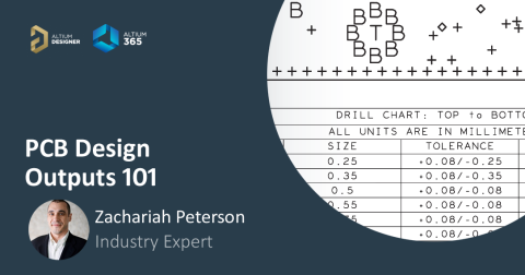


Part 2: PCB Specification Documentation for Your Master Drawing

At a Glance
The master drawing is the most crucial part of your PCB documentation. See how to expertly complete your master drawings to ensure your board is manufacturable.


The master drawing is the most critical part of your design documentation and will convey all of the fine details needed to manufacture your board. While these documentation requirements will change based on the design specifications of your PCB, the overall goal is still to clarify your design intent and avoid any manufacturing delays.
If you would like to skip to different chapters in this series, use the Table of Contents links below:
- Setting Up Your Fabrication Document
- Documenting Your Master Drawing
- Documenting Your PCB for Assembly
- Creating Fabrication and Assembly Drawings In Altium Designer
The master drawing is like the cookbook for your PCB, it includes all the details and instructions on how to manufacture your board. There are specific requirements that you should include in every master drawing.
Master Drawing Class Requirements
Communicating basic information about your design to both your manufacturer and stakeholders mitigates risks of design intent miscommunication. It is highly recommended to utilize the optional blocks that will best fit your particular project’s requirements to facilitate organization of your design documentation. Organized documentation will make it easier for your design intent to connect across your documentation. Now that we have tackled the naming and organization of our documents, let’s take a look at the content of the master drawing.
- Class 1 - All that's needed here is the board layout, which acts as the master drawing. Notes will still need to be added to provide the necessary information to your manufacturer. However, notes are not necessary to pass any kind of Class 1 inspection.
- Class 2 - All Class 2 products require a master drawing that clearly describes the physical dimensions of the board and includes the following details:
- Pattern features not referenced by hole size or location need to be explicitly dimensioned through notes or referenced by a grid system.
- The coating thickness and plating of the board need to be specified.
- If required, quality conformance test markings can be included in the master drawing.
- Class 3 - These types of boards require the most documentation and will need to include the details listed in the table below. Manufacturing processes must also be included, such as drilling, plating or etching.
|
|
|
|
|
|
|
|
|
|
|
|
|
|
|
|
|
|
|
|
|
The information in the table above will be presented in detail in the sections to give you a complete understanding of the requirements for each entry.
Board Details
The board details defines board complexity and structure.
Board Type
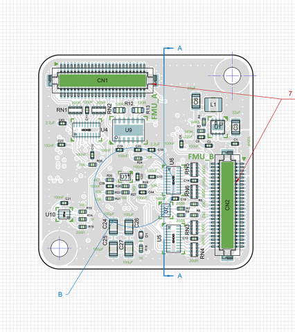
The Continuation Sheet Block is used for sheets other than the first page. A Continuation Sheet Block needs to be placed at the bottom right corner of the page as shown in the example drawing below and should include:
- Type 1 - Single sided
- Type 2 - Double sided
- Type 3 - Multilayer board through-hole components only
- Type 4 - Multilayer board with through, blind and/or buried vias
- Type 5 - Multilayer metal-core board through-hole components only
- Type 6 - Multilayer metal-core board with through, blind and/or buried vias
Board Dimensioning
Board dimensioning is a large subject that warrants its own guidebook, this guide will touch on just a few key points as listed below. For a more detailed and complete look at dimensioning please refer to IPC-C-300[7-3] and ASME-Y-14.57-2].

- You should add a tolerance to each dimension you place.
- Avoid over defining a drawing with unnecessary dimensions.
- Clearly dimension a drawing so that there is only one interpretation.
- Arrange your dimensions to maximize readability.
- Dimension without indicating manufacturing methods, such as what kind of drill bit to use when creating a particular hole.
- Specify the origin to give yourself a reference point.
- Linear dimensions should use a numerical value at its center with arrows in either direction.

Callouts
A callout connects an item with relevant detailed notes. Callouts are generally utilized to bring attention to a special component or when providing notes with limited space. An example of a callout can be seen in Figure 76 below referencing the notes from the title block.

Bow and Twist
The bow and twist notes tell you how flexible or durable the board is by testing how much a board can bend without breaking. Bow and twist requirements should be noted on the master drawing. An example of this can be found in the example notes (note number 11) at the end of this section.
Board Layer Stack
The board layer stack legend includes details about each layer in your board. It is recommended to include the five columns (Layer, Material, Thickness, Type, and Gerber) in every project to keep documentation consistent and streamlined across designs.

Materials
The materials section defines what materials should be mentioned in the notes section of your master drawing and should specify:
- UL requirements
- Laminate type
- Copper foil
The material for the marking inks should also be mentioned. If the marking ink is conductive, then it needs to be properly isolated from the circuitry by spacing it away from other copper or given a coating.
The next time you need to create fabrication documents for your PCB project, use the Draftsman utility in Altium Designer®. This powerful, easy-to-use feature is included in Altium Designer and it will help you speed through the document creation process. When you’re ready to release your board fabrication files and drawings to your manufacturer, the Altium 365™ platform makes it easy to collaborate and share your projects.
We have only scratched the surface of what’s possible with Altium Designer on Altium 365. Take a look at our flexible licensing options for Altium Designer + Altium 365 today.

About Author
Related Resources
Related Technical Documentation
Table of Contents
Design to Release, Without the Friction
- Keep reviews tied to the right version
- Reduce handoff confusion and rework
- Spot sourcing and release risk earlier
- Work solo, share when needed
Get Started
Thank you, you are now subscribed to updates.


