


Introduction to High Density Interconnection

At a Glance
This introduction to Happy Holden's HDI design guidebook gives a comprehensive introduction to high density interconnects.


This article outlines the advanced design approaches and manufacturing processes needed to design the most complex of these PWBs, the high-density interconnects (HDI).
The Evolution of Electronics
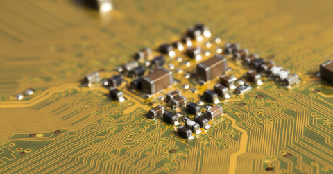
Electronics is a relatively new industry since it has been only 65 years since the transistor was invented. The radio tube was developed nearly 100 years ago but blossomed in WWII, with communications, radar, ammunition fusing (especially the radar-altimeter electronic fusing for the first atom bomb) and has evolved into the world's largest industry. All electronic components must be interconnected and assembled to form a functioning unit. Electronics packaging is the technology where we integrate the design and manufacturing of these interconnections. Since the early 1940s, the basic building platform of electronic packaging is the printed circuit board (PCB). This Guidebook outlines the advanced design approaches and manufacturing processes needed to design the most complex of these PWBs, the high-density interconnects (HDI), as illustrated in Figure 1.
This chapter introduces the basic considerations, the main advantages, and the potential obstacles that must be accounted for in the selection of the high-density interconnection methods. Its main emphasis is on the interconnections and wiring of components. The focus is on density and the potential effects that the selection of various HDI board types and design alternatives could have on the cost and performance of the complete electronic assembly.
As printed circuits became more commonplace since the early 50s, the density and complexity of interconnects have increased quickly, but not as much as the last ten years. Conventional printed circuit technology is capable of meeting most of today’s requirements. Yet, there is a growing group of products referred to as “High Density Interconnects” (HDI for short) that are used to create still denser interconnect, and it is these that are the subject of this Guidebook.
Interconnect Trends
Drivers for higher-density interconnection come under three headings; platforms, performance, and parts:
Platforms
With fast-growing markets for products such as mobile phones, digital appliances, and wearable computers, all of which represent new opportunities. HDI makes possible electronics becoming smaller and lighter.
Performance
With decreased semiconductor rise-times, and more RF and microwave communications, at frequencies up to 80 GHz in some telecom’s areas.
Parts
The evolving silicon technology of smaller transistors and its faster rise-times leads to the challenge to provide more leads in a smaller footprint, which equates to more connections per unit area.
All these trends create a demand for denser interconnects, with smaller trace and gap dimensions, smaller vias, and more buried vias. While this is not necessarily accompanied by a change in board design practices, conventional constructions can reach their limits and the design of HDI constructions require rethinking of design strategies.

FIGURE 1. Electronics have evolved in density from the 1940s to the current state of high-density interconnects that include 3D stacking and embedded components.
HDI Multilayer Platforms
HDI is such a large and growing PWB application market, that there are at least three (3) different HDI Platforms that make it up. These four platforms are 1. Substrates & Interposers modules; 2. Portables; and 3. High performance.
Substrates & Interposers Modules
This technology is used for flip chip or wire bondable substrates. Microvias allow the increased density needed to escape from the high-density flip chips. The dielectric materials are the newer engineered films. A typical example is seen in Figure 2. The modules are small substrates that may have their ICs wire bonded, flip-chipped or TAB mounted or may use fine-pitch CSPs. The discrete components are typically very small, like 0201 or 01005s, and may even be embedded. The design rules are usually coarser than the single IC substrate, since the module may be larger than a single IC package.
Portables
Portables and miniaturized consumer products are the leading edge in HDI Technology. The dense designs offer small form factors and very dense features including micro-BGA and flip chip footprints. The largest application is currently mobile phones. A typical mobile phone product (Motorola MicroTack and the Apple iPhoneX) is seen in Figures 3.
High performance
This technology is used for high layer count boards with high I/O or small pitch components. A buried via board is not always necessary. The microvias are used to form the escape area of dense components (high I/O, micro BGA). Dielectric is reinforces-resin coated foil, reinforced prepregs and cores and high-performance laminates. A typical example is seen in Figure 4. A possible 4th platform to be developed is ‘embedded components’ seen in Figure 5.

FIGURE 2. High-density modules for a. Flip chip substrates and b. Telecom

FIGURE 3. Ever increasing complexity and density characterize the HDI boards used in mobile phones from 1994 through the present day.
 optical network controller. Construction is of low-loss laminates and uses a 1+6+1 HDI structure.")
FIGURE 4. A high reliability telecom board for a triple OC-192 (10 Gb/s) optical network controller. Construction is of low-loss laminates and uses a 1+6+1 HDI structure.

FIGURE 5. The typical usage of microvias to connect various embedded capacitors and
Resistors
Alt Text: Screenshot of microvias to connect various embedded capacitors and
Resistors)
Performance Improvements
When performance improvements are required for PWBs, HDI is the leading contributor. In addition to making the PWB smaller, lighter, and thinner, it will have superior electrical performance. Some of these improvements are:
• Order of magnitude lower via electrical parasitic
• Minimal stubs
• Stable voltage rail
• Removal of decoupling capacitors
• Lower crosstalk and noise
• Much lower RFI / EMI
• Closer ground planes
• Opportunities for distributed capacitance (PWR/GND)
• Surface ground planes w/via-in-pads cut emissions and radiation
As semiconductor fabs reduce the size of their devices, the physics allows faster rise / fall times. This manifests itself in higher-frequency performance. But with smaller devices comes many more on a chip and higher heat dissipation. With a reduction in power supply voltage to minimize the power dissipation, what results is to increase the sensitivity of circuits to various forms of noise and loss of signal strength. High-performance laminates have always been one of the requirements. Additionally, improved processes for microvias fabrication also improve high-frequency performance.
Microvias have nearly 1/10 the parasitics of THs. Test Vehicle structures can validate the lower inductance in microvias, and when combined with low-inductance decoupling capacitors, and via-in-pads, show the merits of noise reduction, especially for high-speed logic.
Access to Advanced Components (parts)
The semiconductor industry is the primary driver for electronics. Smaller gate geometries and greater total gates allow more functions to be performed – and faster. With larger wafers, the prices continue to tumble.
IC packaging, say a 0.80- and 0.65-mm. pitch device, benefit from PCB technologies like HDI, but the use of 0.8 mm pitch and smaller devices is where HDI really begins to provide advantages. The blind vias save room on inner layers and have reduced via lands, as well as making possible via-in-pads. Typical of these devices is the 953 pins, 0.65mm pitch, Digital Signal Processor (DSP) seen in Figure 6a or the 498 pins DSP shown in Figure 6b. The other new components becoming more widespread are ones with very high pin counts of around 600 to 2500 pins, even at 1.00- and 0.8-mm pitches. Although some of these are telecom digital switches (Figure 6c), the vast majority are the new field programmable gate arrays (FPGAs). Current products from Actel, Infineon, Xilinx and Altera have packages with 456, 564, 692, 804, 860, 996, 1020, 1164, 1296, 1303, 1417, 1508, 1696 and 1764 pins. FPGAs of greater than 2000 pins are being designed!

FIGURE 6. a. Fine-pitch devices such as these 953 pins - 0.65 mm pitch microprocessor, b. the 498 pin 0.5mm DSP device or c. the 480 pin @ 0.4 mm controller, even the d. 182 pins @ 0.25 mm require microvias. e. The 2577 pin - 1.0 mm pitch digital switch now require microvias in order to connect them on a printed circuit.
The HDI Opportunities
Other benefits of using HDI technologies can come from the ease of design resulting in Faster Time-to-Market and its Improved Reliability.
Faster Time-to-Market
The faster time-to-market comes about because of easier placement of components using blind vias or via-in-pads. Other design efficiencies come about because of smaller spacing, improved BGA breakouts, boulevards routing (see Chapter 4), and ease of auto-routing using blind/buried vias over through-hole vias. The overall system design times can be reduced because of the improved electrical performance of blind vias instead of TH vias, fewer respins will be required because of signal integrity and noise reduction.
Improved Reliability
Extensive reliability testing was performed by the IPC-ITRI in the late 1990s about the reliability of microvias. [1] Other groups (like HDPUG & NASA-JPL) have also produced reports on the superior reliability of small-blind vias over TH vias. [2] Understanding ‘WHY’ is quite simple! The via aspect ratio (AR-depth to diameter ratio) is less than (6:1 (+) that go as high as 20:1. This is a result of the thin materials and low Z-Axis TCE materials used in HDI (see Chapter 2). HDI materials are numerous and exceed multilayer laminate in variety, thus they are covered by the IPC Standard IPC-4104A and not IPC-4101B. If the blind vias are properly drilled and plated, then they will perform with many times the thermal cycle like typical THs (see Chapter 6)
The thin HDI materials are thus well suited for thermal heat transfer and this is also covered in the IPC HDI Design Standards, IPC-2226.
Lower Cost
Chapters 4 and 5 will discuss in detail, the improved design process for HDI PWBs. Properly planned and executed, an HDI multilayer can be less expensive than the TH board alternative. As illustrated in Figure 4, the Benchmark of a high-speed, controlled impedance 14-layer TH multilayer to an 8-layer HDI multilayer. By fully utilizing the Secondary Side of the PWB, 40% less area was required to connect all the components, in addition to 6 fewer layers.
Predictability or “What Will It Cost?” and the Need For Design Models
Predictability
Customers need to know the HDI stackup, design rules, and PRICE, BEFORE starting the project or board design.
Fabricators can quote the design AFTER it is designed, but without the numbers up front - no one can afford the time to run down a blind alley. The concept that "Microvias cost more!" is one of not knowing how to properly design an HDI board.
One of the benefits of Benchmarking HDI for the last 37 years, was the TH versus HDI Trade-Off chart seen in Figure 7. The Price / Density Comparison. The two key variables are RCI, a comparison currency, normalized to the actual price of an 8-layer multilayer and DEN, the average number of pins on a board divided by the length and width of the board.
 and DENsity predictor (pins/sq. inch) provides a quick comparison of TH layers (column A) to equivalent HDI structures (columns B – G).")
FIGURE 7. TH versus HDI Price / Density Comparison. The Relative Cost Index (RCI) and DENsity predictor (pins/sq. inch) provides a quick comparison of TH layers (column A) to equivalent HDI structures (columns B – G).
The RCIs in the matrix is the ‘Basis’ numbers (or minimums) for costs. But the ‘Ceiling’ number for a range is out of our ability to calculate or set up at this time. It all depends on the various factors in the design. Yields are very sensitive to min. diameter, annular rings, min. trace and spacing, material thicknesses, total number of holes and their density. Other cost factors such as final finish, hole filling, and tolerances will affect the price. I have added a column for “Density” (DEN). This is the Maximum Number of Electrical Connections (called ‘pins’) per square inch of surface (for both sides). The dashed lines are “Equivalent” PCBs. So, as an example, an 18-Layer TH (through-hole-column A) board with an average of 100 ‘pins’ per sq. in could have been designed as a 10-layer HDI board (1+8+1-column C) because it can handle 210 ‘pins’ per sq. in (p/si). Or, it could have been designed as a 6-layer HDI board with 2+2+2 (column E, also 200 p/si).
The RCI does not show the “Absolute” cost savings in this example. The “Relative” cost saving is 28.1% for the 10-layer and 20.5% for the 6-layer HDI ‘equivalents’. But a smaller board could result in more boards per panel and the ‘PRICE” would be even lower than the above numbers. In the range of 8L to 18L, the HDI boards, especially the 2+N+2 are NOT the equivalent of 8L to 18L TH boards, they represent boards with 12X- 20X the density of TH boards.
This Matrix is based on FR-4. This has two important implications. The TH RCI scale (from 4L – 16L) represents competitive pricing set by China. This scale is depressed compared to the HDI pricing. So the HDI pricing, if equal or lower, is very competitive. If the material of construction is NOT FR-4, but a more expensive, low Dk or low Dj material, then the savings from HDI will be MUCH LARGER as you reduce layers!
About Author
Related Resources
Related Technical Documentation
Table of Contents
Design to Release, Without the Friction
- Keep reviews tied to the right version
- Reduce handoff confusion and rework
- Spot sourcing and release risk earlier
- Work solo, share when needed
Get Started
Thank you, you are now subscribed to updates.