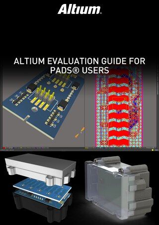
EBook: HDI PCB Design and Manufacturing Guide

The major trend in the electronics industry is miniaturization, where more features and more complexity are packed into a smaller footprint and less board space. High density interconnect (HDI) PCB design is the manifestation of miniaturization at the circuit board level, where smaller components and higher density force changes in design practices and manufacturing processes. HDI PCBs are heavily rules-driven, with most of the rules involved imposed by HDI manufacturing processes. Understanding and following these rules will help ensure a new product can be fabricated and assembled with a high yield.
In this e-book, readers will receive an in-depth look at HDI PCB design and the standard HDI manufacturing processes. Much of this information has been providedby Happy Holden, widely regarded as the godfather of HDI, and a the seminal textbook BGA Breakouts and Routing: Effective Design Methods for Very Large BGAs, by Charles Pfiel, This includes an overview of the materials used in HDI PCBs and the processes used to produce them, as well as some of the constraints that impose particular rules on PCB designers. Covered topics include:
- An overview of the important characteristics of HDI PCBs
- The primary sets of materials used in HDI PCB stackups
- An introduction to the design and manufacturing process for HDI boards
- Important acceptance requirements for manufactured HDI products
Click the PDF above to read more about HDI PCB design and how to navigate the manufacturing process. You can also read the original, full-length content here:
What's Different in HDI?
Introduction to High Density Interconnects
11 HDI Materials You Need to Know
Design Basics for HDI and the HDI PCB Manufacturing Process
HDI Quality and Acceptability Requirements
References:
- Pfeil, C. BGA Breakouts and Routing: Effective Design Methods for Very Large BGAs. Mentor Graphics: 2010.
- Coombs, C. F., and Holden, H. T. Printed Circuits Handbook: Seventh Edition. McGraw Hill: 2016.

