Exploring Semi-Additive Processes (SAP) in Ultra HDI PCB Fabrication

As PCB technology continues to evolve, new manufacturing techniques like ultra-high-density interconnect (UHDI) PCB fabrication are unlocking incredible possibilities. Among the most transformative advancements are semi-additive processes (SAP) and modified semi-additive processes (mSAP), which enable the creation of finer traces and spaces beyond what traditional subtractive etching can achieve. These innovations are pushing the boundaries of PCB design, making it possible to fabricate intricate circuits with unprecedented precision.
In the context of PCB fabrication, semi-additive processes (SAP) offer a departure from traditional subtractive methods by allowing traces and spaces that were previously unachievable—well below the 2-mil threshold possible with subtractive etching. SAP processes enable fabricators to add conductive material, like copper, to form circuitry rather than etching it away. This technique, paired with advanced materials, opens the door to ultra-fine feature sizes that support the next generation of electronics, including high-performance, miniaturized devices.
Key Advantages of Semi-Additive Processes in PCB Fabrication
Extreme Miniaturization
One of the most exciting opportunities with SAP and mSAP technologies is the ability to drastically reduce PCB footprint. With trace and space dimensions shrinking to sub-micron levels, designers can dramatically reduce the size of the overall electronic system or, alternatively, use the freed-up space to integrate additional components, such as larger batteries or enhanced functionality. This is particularly critical for devices where space is at a premium, such as smartphones, wearables, and IoT devices.
Simplified Layering and Enhanced Routing Efficiency
Another significant benefit of these processes is the potential reduction in the number of layers required in a PCB design. For components with tight-pitch ball grid arrays (BGAs) or even standard designs, the ability to route complex signals on fewer layers can reduce both cost and complexity. Fewer layers also mean fewer micro-vias and lamination cycles, leading to shorter manufacturing times and higher overall yields. The ability to simplify the layer structure while maintaining or improving functionality is a huge win in terms of both reliability and performance.
Improved Signal Integrity and Precision
While miniaturization and layer reduction are tangible benefits, SAP processes also significantly enhance electrical performance. One of the most critical improvements is in signal integrity. Because semi-additive processes rely on precise imaging techniques rather than the broader subtractive etching process, they allow for finer control over trace width and spacing. This results in tighter impedance control and reduced signal degradation, making these technologies ideal for high-speed digital and RF applications.
Semi-Additive vs. Subtractive Etching: A Brief Overview
Traditional subtractive etch processes start with a copper-coated laminate, and the circuit pattern is formed by etching away the unwanted copper. The process, while effective, has limitations in achieving fine traces and spaces due to the copper thickness and the etching methods used.
In contrast, semi-additive processes begin with a very thin layer of copper or no copper at all in the case of pure additive methods. Copper is then selectively added to create the desired pattern, with only a thin seed layer requiring removal. This precision allows for much finer features, with traces as narrow as 25 microns (or below), depending on the imaging capabilities of the fabricator.
Modified Semi-Additive Processes (mSAP)
Modified semi-additive processes (mSAP) are an extension of SAP, often used in the high-volume production of consumer electronics like smartphones. The key difference lies in the starting copper layer—mSAP starts with a slightly thicker foil, leading to slightly less refined trace profiles. While mSAP allows for excellent feature sizes, they typically range in the 30-micron trace/space range, with traces having a more trapezoidal shape due to the thicker starting copper.
Despite these differences, mSAP still enables much finer features than traditional subtractive methods and is considered a bridge between standard PCB and advanced substrate-level manufacturing techniques. This approach is critical in cost-sensitive, high-volume applications.
Substrate-Like PCBs (SLP) and the Future of Ultra HDI
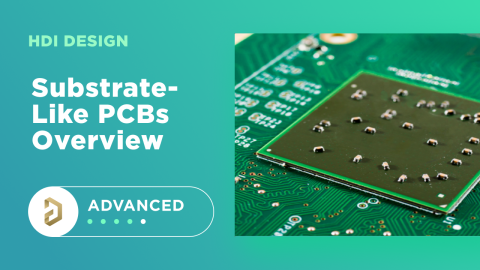
A term frequently used in this space is "substrate-like PCBs" (SLP), which refers to circuit boards built with additive or semi-additive processes. SLPs allow for fine-feature capabilities that approach the precision of semiconductor substrates but on much larger PCB panels. This is particularly advantageous for applications requiring miniaturization without sacrificing the cost and scalability benefits of traditional PCB manufacturing.
Typical SAP and mSAP Process Flow
For both SAP and mSAP, the process flow follows similar steps:
- Photoresist Application – A layer of photoresist is applied to define the circuit pattern.
- Photoresist Imaging – The photoresist is exposed to UV light, which defines the areas where copper will be added.
- Electrolytic Copper Plating – Additional copper is selectively plated onto the patterned areas.
- Photoresist Stripping – The remaining photoresist is stripped away, leaving behind the copper traces.
- Etching – For mSAP, the copper seed layer is etched to complete the process, with SAP requiring only minimal etching.
Because SAP begins with an ultra-thin copper layer (as thin as 1.5 microns or less), the final traces have vertical sidewalls, allowing for extremely fine features, whereas mSAP typically leaves traces with more trapezoidal profiles due to its thicker starting copper.
Partnering with Your PCB Fabricator for Success
The key to leveraging these advanced fabrication methods lies in close collaboration with your PCB manufacturer. As John Johnson, Director of Quality for American Standard Circuits, notes, “Designers must collaborate with fabricators to fully understand the trade-offs and capabilities of various semi-additive processes. A 'it depends' approach to design rules is common, and working together ensures optimized performance, manufacturability, and cost, allowing designers to maximize the potential of ultra-HDI technology." In this collaborative approach, both designer and manufacturer play an essential role in optimizing designs for the unique capabilities of SAP and mSAP, ultimately leading to more efficient, powerful, and reliable electronic systems.
