What's HDI? Design Basics and the HDI PCB Manufacturing Process


As the world of technology has evolved, so has the need to pack more capabilities into smaller packages. PCBs designed using high-density interconnect (HDI) techniques tend to be smaller as more components are packed in a smaller space. An HDI PCB uses blind, buried, and micro vias, vias in pads, and very thin traces to pack more components into a smaller area. We’ll show you the design basics for HDI and how Altium can help you create a powerful HDI PCB design.
High density interconnect (HDI) printed circuit design and fabrication started in 1980 when researchers started investigating ways to reduce the size of vias in PCBs. The first production build-up or sequential printed boards appeared in 1984. Ever since that time, designers and component manufacturers always look for ways to pack more functions on a single chip and a single board. Today, HDI board design and fabrication are codified in the IPC-2315, IPC-2226, IPC-4104, and IPC-6016 standards.
When planning an HDI PCB design, there are some design and manufacturing challenges to overcome. Here is a short list of challenges you may run into when designing an HDI PCB:
- Limited board workspace area
- Smaller components and tighter spacing
- Larger number of components on both sides of PCB stackup
- Longer trace routes creating longer signal flight times
- More trace routes required to complete the board
With the right set of layout and routing tools built on a rules-driven design engine, you can violate the normal rules in PCB design and create powerful PCBs with very high interconnect density. Working with high-density PCB routing and fine pitch components is easy when you use advanced PCB design software that is built for HDI PCB design. You can create your new HDI board design and plan for the HDI manufacturing process with the world-class design features in Altium.
What’s Different About HDI PCB Design and Manufacturing?
The HDI manufacturing process differs from the traditional PCB manufacturing process in a few simple yet important ways. An important point here is that fabricator limitations will constrain design freedom and will set limits as to how the board can be routed. The use of thinner traces, smaller vias, more layers, and smaller components can still be accommodated in your design software, but accommodating design for manufacturing (DFM) requirements means taking advantage of automation in your design software. The exact DFM requirements depend on the manufacturing process and materials used to build the board. DFM requirements also become important when we consider reliability requirements.
Material selection needs to answer these questions:
- Will the dielectric use chemistry be compatible with current chemistry used by core substrate material?
- Will the dielectric have acceptable plated copper adhesion? (Many original equipment manufacturers [OEMs] want >6 lb./in. [1.08 kgm/cm] per 1 oz. [35.6 µm] copper.)
- Will the dielectric provide adequate and reliable dielectric spacing between metal layers?
- Will it meet thermal needs?
- Will the dielectric provide a desirable “high” Tg for wire bonding and rework?
- Will it survive thermal shock with multiple SBU layers (i.e., solder floats, accelerated thermal cycles, multiple reflows)?
- Will it have plated, reliable microvias?
There are nine different general dielectric materials used in HDI substrates. IPC slash sheets like IPC-4101B and IPC-4104A cover many of these, but many are not yet specified by IPC standards. The materials are:
- Photosensitive liquid dielectrics
- Photosensitive dry film dielectrics
- Polyimide flexible film
- Thermally cured dry films
- Thermally cured liquid dielectric
- Resin-coated copper (RCC) foil, dual-layer and reinforced
- Conventional FR-4 cores and prepregs
- New ‘spread-glass’ laser-drillable (LD) prepregs
- Thermoplastics
The HDI PCB design process is shown below. Routing efficiencies for HDI are dependent on stackup, via architecture, parts placement, BGA fanout, and design rules. The most important parts of planning your HDI layout are to consider your trace width, via size, and placement/escape routing for BGA components.
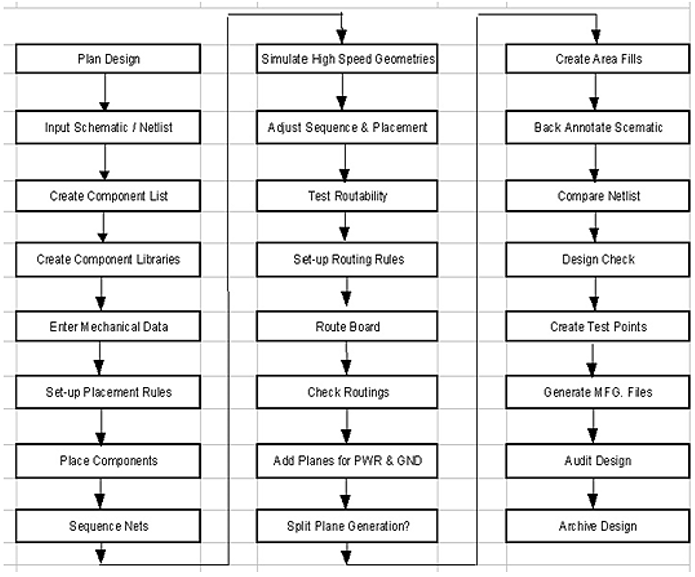
General overview of the HDI PCB design and layout process.
Always check with your board house to determine their fabrication methods for HDI PCB manufacturing. You’ll need to determine the limits of their fabrication methods as this will influence the feature sizes you can place in your layout. The ball pitch on BGA components will determine the via size you need to use, which then determines the HDI manufacturing process required to create the board. A central feature of your HDI PCB is microvias, which need to be precisely designed to accommodate routing between layers.
Overview of HDI PCB Design and Manufacturing Processes
There are a number of steps involved in the typical PCB manufacturing process, but HDI PCB manufacturing uses some particular steps that may not used in other boards. The HDI board design process starts like many other processes, where the
- Determine the layer count required to route all signals, either by using the largest BGA component on the board or by using the interface + direction count from the largest IC on the board.
- Contact your fabrication house to select materials and obtain dielectric data to create your PCB stackup.
- Based on layer count and thickness, determine the via style that will be used to route signals through inner layers.
- Perform a reliability assessment if relevant, to verify that the materials will not stress interconnects to fracture during assembly processing and operation.
- Determine design rules based on fabricator capabilities and reliability requirements (need for tear drops, trace widths, clearances, etc.) to ensure reliable manufacturing and assembly.
Stackup creation and determination of design rules are the critical points as they will determine ability to route the board and reliability of the end product. Once these points are completed, a designer can implement their fabricators DFM requirements and reliability requirements as design rules in their ECAD software. Doing this on the front-end is very important and it will help ensure the design is reliable, routable, and manufacturable.
Design Your Feature Size to Satisfy HDI DFM Requirements
Although DFM requirements relating to clearances in an HDI PCB are quite stringent, these can be accommodated by taking advantage of your design rules in your PCB design software. Some of the important DFM requirements to gather before layout and routing include:
- Trace width and spacing limits
- Annular ring and aspect ratio limits, especially for high reliability designs
- Material system used in the board to ensure controlled impedance in the required stackup
- Impedance profiles for the desired stackup or layer pairs if available
Your design tools are critical for designing your HDI circuit board to satisfy these DFM requirements. Routing impedance controlled traces in your HDI PCB is quite easy with the right set of design tools. You simply create an impedance profile and define your desired trace width while keeping your manufacturer’s DFM guidelines in mind. The online DRC engine in your routing software will check your routing as you create your HDI layout. Make sure you get a complete set of specifications for your fabricator's process to ensure you've taken into account all the relevant HDI DFM rules.
Types of Vias in HDI PCB Routing
The image below shows the typical via styles that are used in HDI PCB layout and routing. These via styles have low aspect ratio of )(ideally) less than 1, although some manufacturers may provide reliability claims up to aspect ratios of 2, including for stacked microvias. In the center of the PCB stackup is a conventional buried via to provide a connection through the thicker core layer; this inner layer buried via can have a larger aspect ratio as will be mechanically drilled with somewhat . Once the layer count and dielectric thicknesses are determined, the designer can design vias against the aspect ratio limits listed above. Obeying these aspect ratio limits on microvias is an important part of reliability, particularly as these boards pass through reflow, or when deployed in an environment with repeated thermal/mechanical shocks and cycling.
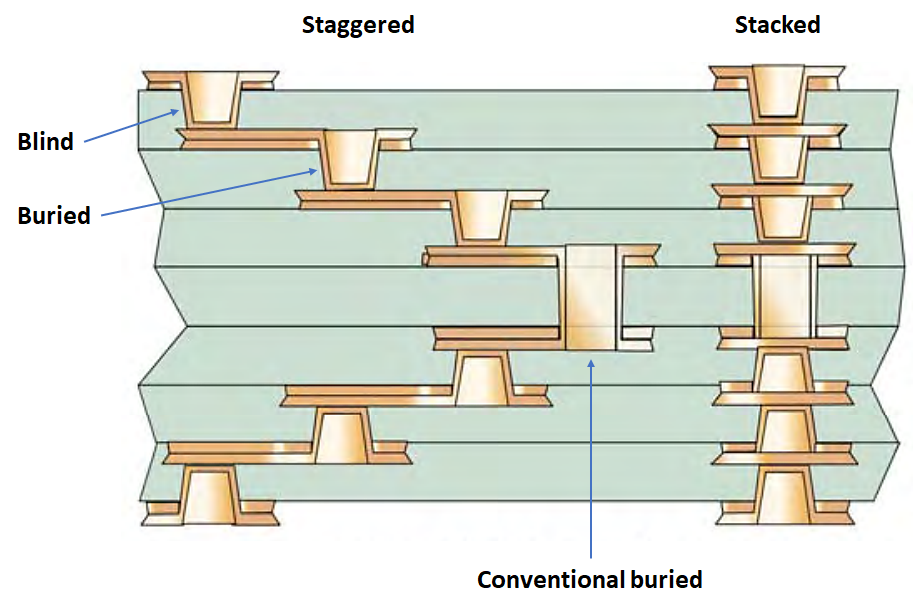
Sequential Buildup
The sequential lamination process is predominantly used to build an HDI stackup construction in a layer-by-layer manner. In general, this technique can be used for any multilayer PCB, but it is particularly important for HDI. This is because the high density, very thin dielectrics are formed in individual layers around a thick core, so lamination will happen in multiple steps to build the stackup. The sequential lamination process. This consists of the following steps:
- Photoresist deposition and exposure: This is used to define areas to be etched, which will leave behind a pattern of conductors on the laminate.
- Etching and cleaning: The current industry standard etchant is a ferric chloride solution. After etching, the leftover photoresist can be reclaimed and the resulting conductor pattern is cleaned.
- Via formation and drilling: Vias need to be defined using mechanical or laser drilling. For high via density, the via holes can be removed chemically.
- Via metallization: Once vias are defined, they are metallized to form a continuous conductive interconnect.
- Buildup: Layers are stacked in multiple lamination cycles to build the stackup before outer layer processing.
A flow chart showing the buildup process can be found in the Metalization section below.
Via Formation in HDI
HDI PCBs will require interconnects that typically hit the lower limit of the via size that can be placed in a PCB with mechanical drilling. Once via holes get smaller than 6 mils, an alternative via formation process is needed to place microvias between layers. As filled plated microvias are a standard feature on HDI PCBs, they can be used in a via-in-pad design approach to help increase density. Using via-in-pad is an easy way to pack more components into a design as they provide a direct connection from a component lead into an internal layer.
Whenever there are reliability concerns regarding microvias, a near-pad technique can also be used, where a very small trace section comes off from a pad and touches the microvia. This completes the connection to an internal layer and provides a larger breakout channel should drill wander create some deviation from the desired drill hit location.
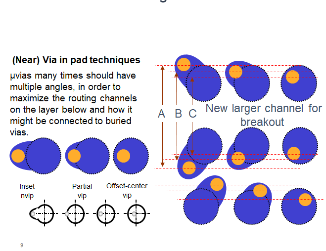
Via-in-pad design styles for HDI PCBs.
Metalization
During the sequential lamination process, each layer in an HDI PCB will go a via metalization, fill, and plating process. The resulting vias must be void-free in the internal body with sufficient wrap plating around the neck so that cracking can be avoided during reflow cycles and during operation. There are four via metallization processes that are used in HDI manufacturing. These methods are:
- Conventional electroless and electroplating copper
- Conventional conductive graphite or other polymers
- Fully and semi-additive electroless copper
- Conductive pastes or inks
Larger vias can be drilled, but the costs eventually exceed laser drilling costs with lower throughput as a slower drilling speed is required. Laser drilling is by far the most popular microvia hole formation process, but it is not the fastest via formation process. The chemical etching of small vias is the fastest, with an estimated rate of 8,000 to 12,000 vias per second. This is also true of plasma via formation and photovia formation.
In laser drilling, a high fluence beam is used to place a hole in a PCB laminate. Lasers are capable of ablating dielectric material and stopping when intercepting the copper circuitry, so they are ideally suited for creation of depth-controlled blind vias. The wavelengths for laser energy are in the infrared and ultraviolet region. A beam spot size as small as approximately 20 microns
If the vias in the board are wide enough to drill, a controlled drilling step may be used to place vias. This requires an intermediate sequential lamination step to bond two layers of the board, followed by drilling and plating to define the via barrel, connection to the inner layer, and landing pad on the upper layer. These vias might also be filled before the next sequential lamination step (if they are on the inner layers), or they could be left un-filled if kept on the outer layers.The overall drilling and sequential process is shown below.
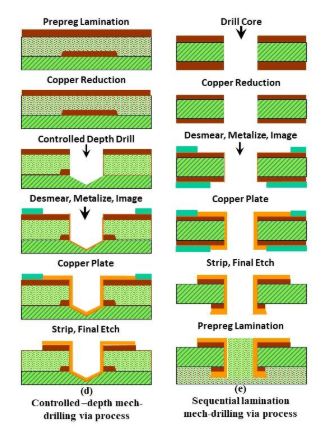
Microvia drilling and metalization processes in an HDI manufacturing process.
Getting Your Board Into the HDI Manufacturing Process
HDI PCB processes are more advanced than traditional rigid PCB processing steps, but they still use the same set of fabrication data you use for a typical rigid PCB. Once you’ve finished your HDI PCB layout and it’s passed a DFM review, it’s time to prepare deliverables for your fabricator and assembler. The unified design environment in Altium takes all your design data and uses it to create Gerbers/ODB++/IPC-2581 fabrication files, drill tables, a bill of materials, and assembly drawings for your new HDI PCB.
When you’re looking for the best software package for HDI PCB design, layout, and manufacturing, use the complete set of design tools in Altium. The integrated design rules engine and Layer Stack Management give you everything you need to create your bare HDI circuit board, calculate impedance values, and account for copper roughness in your PCB material system. When you’ve finished your design, and you want to release files to your manufacturer, Altium makes it easy to collaborate and share your projects.

