


EMI-Reducing PCB Shielding Techniques For Your Designs

At a Glance
When strong noise is a challenge in your design and it is preventing compliance with radio emissions regulations, some shielding techniques can help.


Whenever a designer or design team has trouble passing pre-compliance testing or full EMC testing with an accredited lab, they probably start searching for EMI shielding solutions. EMI shielding can be applied at multiple levels, such as targeted individual circuits, placed throughout the entire PCB, or placed around the enclosure. Cable shielding is another option designers may consider, both with off-the-shelf shielded cables or adding shielding to custom-designed cable assemblies or harnesses.
However, before adding shielding to a PCB assembly or enclosure indiscriminately, you should first ask yourself: Will a PCB redesign fix the problem that results in the requirement for shielding?
Many times, the need for shielding can be completely eliminated by analyzing and changing the PCB layout. It is also worth looking at specific circuits and identifying changes in order to reduce EMI and potentially eliminate the need for shielding. If you have performed these tasks and still require shielding, or you don't mind the additional materials and assembly costs for shielding, then there are some great options that can be used on the PCB and in enclosures to provide shielding from EMI.
EMI Shielding Techniques Overview
There are some simple yet effective ways to apply EMI shielding techniques. There are some component and materials companies that supply specialty electromagnetic shielding materials targeting a range of frequencies. When initial methods like filters and best layout practices fail, you can use the following features in your PCB layout:
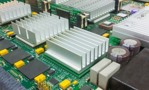
- Metal circuit board shielding cans can be custom fabricated and mounted around noisy circuits to suppress excessive electromagnetic radiation.
- Elastomer electromagnetic shielding materials can be used to target specific components and connectors in the PCB layout to suppress electromagnetic radiation.
- High electrical conductivity mesh materials can be used as a flexible alternative to rigid shielding cans, particularly in flex or rigid-flex boards.
- Replacing separated/star ground with uniform ground planes provides multiple grounding points and helps ensure conductive circuit board shielding materials can be grounded easily.
- Ferrite beads, rods, and plates can be used as targeted EMI filters when conventional filter circuits fail.
These are some simple methods and components that can be accessed from various vendors and incorporated into your PCB design software. However, you should still make sure to implement some best practices in your PCB layout to ensure the design can pass EMC tests.
PCB Shielding Components and Materials
Aside from PCB design-level solutions like a chassis guard ring or copper pours, the most common EMI shielding component is metal shielding enclosures that mount to the circuit board. These very thin sheet metal enclosures solder onto the PCB in a reflow process, so they can be quickly and reliably placed on an SMT line.

Metal shielding cans come in standardized form factors with a specific footprint, headroom, and shape. Forward-looking design teams can accommodate the headroom and component placement limitations with the standardized shielding cans. Unfortunately, shielding cans are often considered at the end of a design when there is an EMI problem and the can is a candidate to add to the PCB. This could force a lot of placement changes for some components, and it may require BOM changes to accommodate the headroom inside the shielding.
When this occurs, designers may instead try to use custom shielding cans on the PCB. This is not a completely prohibitive process as shielding cans are essentially bent sheet metal. Building vendors may be willing to produce a custom solution that is cost-effective up to a certain volume. At very high volumes, shielding cans may need to be stamped rather than cut or milled, which will further decrease unit cost for these components. For custom solutions, contact shielding can vendors like Laird and request a consultation for a custom component.
Enclosure-Level EMI Shielding Techniques
When board-level EMI shielding measures are ineffective, either because they cannot address a high-frequency range or because EMI is too intense, such as you might see in high current switching regulators. In this case, enclosure-level EMI shielding techniques can be used. These include:
- Applying metal cans or mesh materials to mating surfaces to close gaps in an enclosure
- Applying flexible elastomer materials to mating surfaces in harnesses and pipe fittings
- Applying grounded mesh or metal sheets in a plastic enclosure to create a lightweight electromagnetic shielding cage
- Using a high conductivity gasket EMI shielding material on circular mating surfaces
These solutions are simple, yet they are effective for preventing electromagnetic radiation from escaping an enclosure if EMI is a problem. These solutions tend to be broadband up to high frequency, and they tend to be cost-effective in that they generally don’t require modifying the PCB layout or require minor changes to an enclosure. All of these circuit board shielding, enclosure, and board-level requirements need to be communicated to the fabrication and assembly teams with standard documentation to ensure successful manufacturing.
Metalized Enclosures
Metalized enclosures are an excellent option for protecting against stray electromagnetic fields and external environmental factors. Once the enclosure is grounded to the PCB, it functions as a conducting plane for ESD and noise currents, as well as blocking electromagnetic waves.
How a metalized enclosure is used will impact the product’s ability to comply with EMC requirements. How the metalized enclosure is connected to the ground depends on:
- If an earth ground connection is present
- If the design has galvanic isolation (e.g., an isolated DC/DC converter)
- If the design has its metalized enclosure exposed to the user
- If the design uses shielded connectors/cables
- If the design has a grounded chassis ring that makes a single connection point to the power supply ground
There are different reasons these grounding schemes would be implemented. For example, when user safety is important (e.g., in medical devices), leakage currents between galvanically isolated grounds or via connector shields are not allowed to reach the user, requiring insulation of the enclosure, filtering, or changing any safety capacitors between the ground/enclosure. To learn more, take a look at the following resources on grounding with mounting holes and metalized enclosures:
- All About Ground Reference and Chassis Ground in Electronics Design
- PCB Grounding Techniques for Plated PCB Mounting Holes
- How to Connect Grounds in an Isolated Power Supply PCB Layout

Shielding Compounds and Gaskets
Shielding compounds are available as one-part or two-part materials which can be applied by hand to an enclosure. Typically, they will be applied to cracks and seams in an enclosure in order to create an absorber for high-frequency radiated emissions. The application of these compounds by hand requires additional assembly work, so they may not be an ideal solution for volume production.
Gaskets are an alternative that play the same role as shielding compounds in that they are intended for absorbing EMI at seams and mating surfaces in an enclosure. They could also be applied on certain surfaces of the PCB which must mate to a mechanical element, although this is less common. Gaskets used in enclosures are generally die-cut films which could be applied with an adhesive. They are lower-cost components that can be custom-designed and can be more easily applied in high-volume assembly.
Another type of gasket material which is used on larger enclosures is a mesh gasket or metallic gasket. These are more common on cabinet enclosures or panelized enclosures rather than small metalized enclosures. Large absorber gaskets are prohibitive on cabinet or panelized enclosures, so metallic gaskets are a more cost-effective solution that is easier to handle. While they can technically be custom-designed for certain panel shapes, it may not be necessary as metallic gasket vendors produce a variety of solutions for enclosures.
One alternative to gaskets which is commonly used on cables is shielding tape. The shielding effectiveness of tapes depends on the thickness of the tape and the type of material used. Tapes are probably not the best option for production hardware, but it can be very useful in prototyping and testing.
EMI shielding tape [Image credit: 3M]
Conformal Coating as an EMI Absorber
Many designers may not be aware, but conformal coatings provide several benefits depending on the coating material type and where the coating is applied. For example:
- Conformal coatings provide moisture and dust ingress protection
- Coatings can be applied selectively using a mask
- Some coatings are reliable up to very high temperatures and will not degrade or flake
- Some coating materials provide low outgassing
- Some conformal coating materials can be electromagnetic absorbers
The last point makes conformal coating materials useful as an EMI solution for radiated emissions from the PCB edge or from circuits on the surface layers at moderate frequencies (~1 MHz and harmonics). Applying a conformal coating to the entire PCBA or through a mask on specific components is possible by hand or it can be performed in a volume production environment.
There is some data illustrating the effect of some conformal coating materials on radiated emissions, specifically from a PDN with significant switching noise. The effect depends on the material’s loss tangent, which brings up two candidate materials that can provide absorption:
- Polyurethane: Df = 0.071 @ 1 MHz
- Parylene C: Df = 0.013 @ 1 MHz
Make sure you verify the RF absorption strength of conformal coat materials with the vendor, although be aware that not all vendors have tested conformal coating materials for these applications. Therefore, pre-compliance testing may be necessary in the lab in order to verify the effectiveness of a specific conformal coating material as an EMI absorber.
Ferrite Cores, Plates, and Chokes
Targeted use of ferrites, particularly in DC systems, can be very effective at reducing EMI at high frequencies. Most designers are familiar with ferrite beads and they tend to apply these in situations where they are never needed or where the ferrite bead creates noise and EMI. However, there are other ferrite materials and components which can be used to target specific sources of EMI:
| Ferrite Type | Description |
|---|---|
| Ferrite chokes |
|
| Ferrite plates |
|
| Ferrite cores |
|
Before applying chokes or cores on signal lines, one must verify that the cores do not create strong insertion loss within the required channel bandwidth. For this reason, cores and chokes are not often used on high-speed signal lines. However, there are ferrite chokes which are rated for specific interfaces and data rates, so they can be quite useful in some situations and may eliminate the need for a core on an attached cable (e.g., in a USB cable or HDMI cable).
What Can You Do in the PCB to Reduce EMI?
In order to accommodate all of the solutions discussed here, some changes to the PCB layout will be required. This could be as simple as adding a component (in the case of chokes) or as complex as changing a circuit design and layout (in the case of shielding cans). Beyond these solutions which add components or external shielding to the PCB, there are additional factors in the PCB design itself which can impact EMI. Some of these include:
- Addition of an edge guard ring and via fence to reduce radiated emissions from the PCB edge
- Placement of copper pour and stitching vias around specific circuits and signals
- Changing the PCB stack-up to bring a ground plane closer to some circuits or signals
- Implement the correct grounding strategy and ties for galvanically isolated circuits
- Reroute certain signals to reduce their return path length and loop inductance
- Change component pinouts to allow for ground pins between signal lines and conductors
- Reroute input power lines to switching converters such that they have higher rail capacitance
These strategies primarily impact radiated emissions and susceptibility, but they are not a guarantee to solve conducted emissions problems. For conducted emissions, particularly those relating to mode currents, the potential solutions listed here need to be invented carefully and in a targeted manner. Testing is often required to identify conducted emissions problems before implementing these solutions.
Whether you need to build reliable power electronics or advanced digital systems, use the complete set of PCB design features and world-class CAD tools offered by Altium. Altium Develop provides the world’s premier electronic product development platform, complete with the industry’s best PCB design tools and cross-disciplinary collaboration features for advanced design teams.

About Author
Related Resources
Related Technical Documentation
Table of Contents
Design to Release, Without the Friction
- Keep reviews tied to the right version
- Reduce handoff confusion and rework
- Spot sourcing and release risk earlier
- Work solo, share when needed
Get Started
Thank you, you are now subscribed to updates.

